A processor can perform millions or billions of operations every second. It can add numbers, compare values, calculate addresses, control loops, call functions, and move data through a program.
Before any of those operations can happen, the processor must obtain the values required by the current instruction.
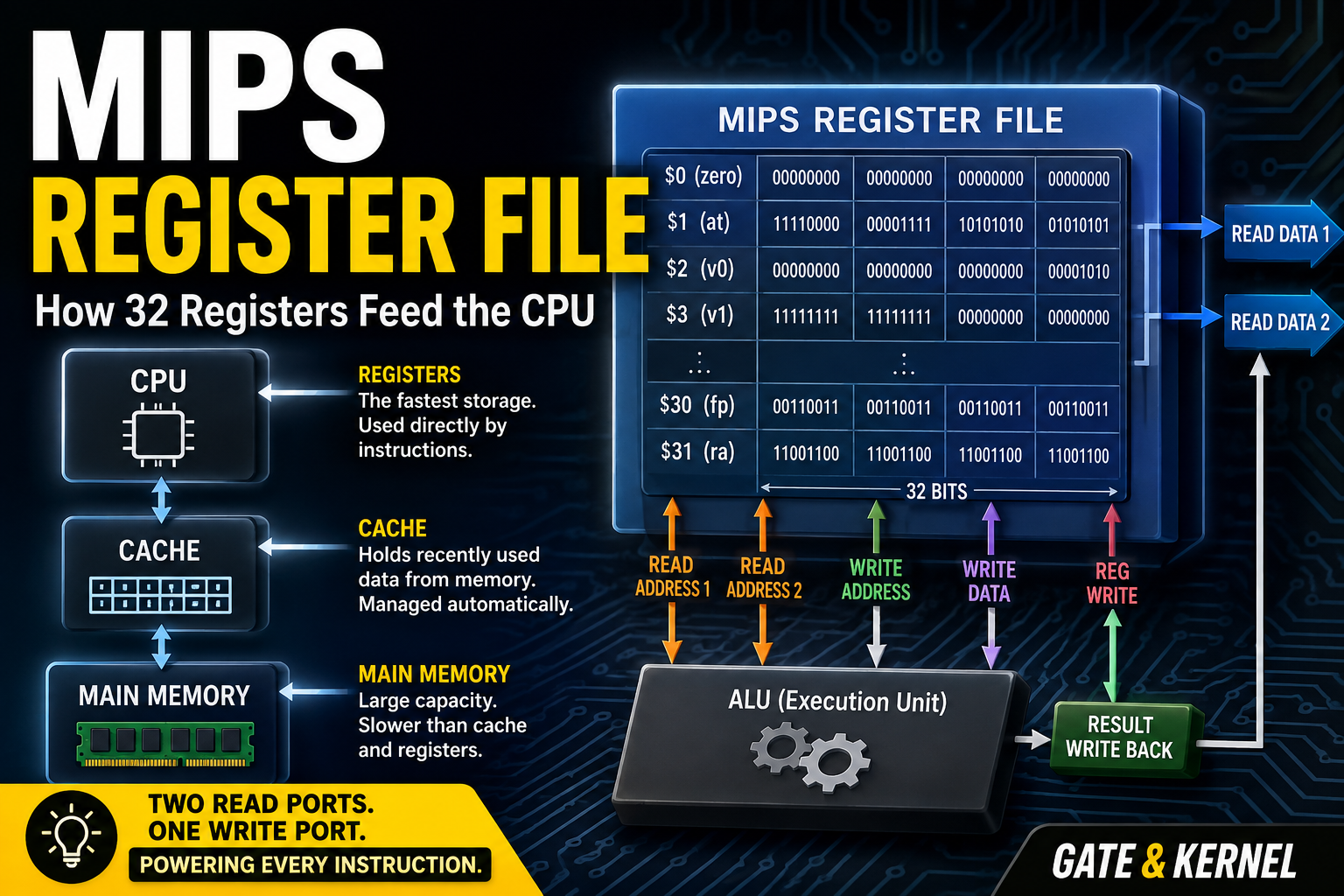
Those values may originally come from memory, but a processor cannot rely on main memory for every simple calculation. Main memory offers a large capacity, but it is much slower than the execution hardware inside the CPU.
The processor therefore keeps its most immediate working values in registers.
In the classic 32-bit MIPS architecture, the programmer-visible integer register set contains thirty-two general-purpose registers. Instructions identify these registers using five-bit register fields.
In a commonly used single-issue teaching datapath, the registers are represented as a register file with two read ports and one write port. This allows an instruction to obtain two source operands and later write one result.
This article explains both sides of the subject:
- What the MIPS architecture makes visible to software
- How a classic textbook register file can implement that behavior
The distinction matters because the instruction-set architecture does not require every physical MIPS processor to use exactly the same internal register-file circuit.
1. What Is a Register?
A register is a small storage location inside a processor.
In MIPS32, each general-purpose register holds a 32-bit value. That value may represent:
- A signed or unsigned integer
- A memory address
- A character or bit field
- A mask used by logical operations
- A function argument
- A return value
- An intermediate calculation result
The bits in a 32-bit register are normally numbered from 0 through 31.
- Bit 0 is the least significant bit.
- Bit 31 is the most significant bit.
Each bit stores either zero or one. Together, the thirty-two bits form one complete binary value.
A single register has very little capacity, but registers are directly involved in instruction execution. They hold the values that arithmetic, logical, branch, load, and store instructions use.
2. Architectural Registers and Physical Hardware
It is useful to separate two related ideas.
Architectural registers
These are the registers visible to machine instructions and software.
The MIPS32 architecture defines thirty-two general-purpose registers, numbered from 0 through 31. An instruction can name these registers as sources or destinations.
Physical register-file hardware
This is the circuit used by a particular processor implementation to provide the required architectural behavior.
A simple MIPS processor may implement the registers as one compact array with two read ports and one write port.
A more advanced processor may use:
- Additional ports
- Multiple banks
- Replicated storage
- Pipeline stages
- Shadow register sets
- Separate register contexts for hardware threads
- Internal physical registers used for register renaming
Software still sees the architectural register set, even when the physical implementation is more complicated.
Throughout this article, register file refers mainly to the classic teaching implementation unless stated otherwise.
3. The Thirty-Two General-Purpose Registers
The classic MIPS32 programmer-visible integer register set contains thirty-two general-purpose registers.
They are numbered:
Register 0
Register 1
Register 2
...
Register 31
Because there are thirty-two possible registers, a register number requires five bits:
2^5 = 32
A five-bit binary value can represent the numbers 0 through 31.
This is why register fields such as rs, rt, and rd in classic MIPS instruction formats are five bits wide.
The instruction supplies a register number. The processor uses that number to access the corresponding architectural register.
This register number is not a memory address. It is a small identifier used inside the processor.
4. What Does “32 × 32 Register File” Mean?
A classic MIPS32 register file is often described as a:
32 × 32 register file
The first number represents thirty-two registers.
The second number represents thirty-two bits per register.
Conceptually, it can be drawn as a table:
Register 0   — 32 bits
Register 1   — 32 bits
Register 2   — 32 bits
...
Register 31  — 32 bits
When a read address identifies one row, the corresponding 32-bit value appears at the read output.
When a write address identifies one row, that register may store a new 32-bit value when writing is enabled.
This table is a useful logical model. A real integrated circuit does not necessarily look like thirty-two separate rectangular registers connected to giant visible multiplexers.
5. Does the Register File Contain Only 128 Bytes?
Thirty-two registers multiplied by thirty-two bits gives:
32 × 32 bits = 1,024 bits
Since eight bits equal one byte:
1,024 bits ÷ 8 = 128 bytes
Therefore, the thirty-two programmer-visible MIPS32 general-purpose registers represent 128 bytes of architectural integer state.
That does not necessarily mean that a real processor contains only 128 physical bytes of register-related storage.
A particular implementation may include:
- Shadow copies of the register set
- Separate register sets for multiple hardware threads
- Pipeline storage
- Test and recovery structures
- Additional implementation-specific registers
The 128-byte figure describes the information capacity of one visible set of thirty-two 32-bit general-purpose registers.
6. Why Did Classic MIPS Choose Thirty-Two Registers?
The number of registers is connected to instruction encoding.
Classic MIPS instructions are 32 bits long. Many instructions must encode:
- One source register
- A second source register
- A destination register
- An operation code
- Additional function or immediate information
Thirty-two registers require five bits per register field.
This provides a practical balance.
More registers could reduce the need to move temporary values to memory, but larger register numbers would consume more instruction bits.
Fewer registers would reduce the size of the register fields, but software would have less fast working storage.
The MIPS design uses thirty-two general-purpose registers while preserving a regular 32-bit instruction format.
7. Register Numbers and Assembly Names
MIPS assembly programmers normally use symbolic register names rather than writing only numerical register identifiers.
For example:
add $t0, $t1, $t2
The symbolic names make the purpose of the code easier to understand.
However, names such as $t0, $s0, $a0, and $v0 are primarily part of software conventions and application binary interfaces.
They do not mean that the underlying registers use fundamentally different storage circuits.
For example:
$t0 = Register 8
$t1 = Register 9
$s0 = Register 16
$sp = Register 29
$ra = Register 31
The assembler converts the symbolic names into register numbers before generating machine code.
The hardware ultimately works with the encoded numbers.
8. Common Register Names in the Classic o32 ABI
The following names and uses are commonly associated with the classic MIPS o32 calling convention.
| Number | Name | Common software use |
|---|---|---|
| 0 | $zero |
Constant zero |
| 1 | $at |
Reserved for assembler-generated code |
| 2–3 | $v0–$v1 |
Function return values |
| 4–7 | $a0–$a3 |
Function arguments |
| 8–15 | $t0–$t7 |
Caller-saved temporary values |
| 16–23 | $s0–$s7 |
Callee-saved values |
| 24–25 | $t8–$t9 |
Additional temporary values |
| 26–27 | $k0–$k1 |
Reserved for kernel use |
| 28 | $gp |
Global pointer |
| 29 | $sp |
Stack pointer |
| 30 | $fp or $s8 |
Frame pointer or saved register |
| 31 | $ra |
Return address |
These uses are software conventions.
The architectural exception is register 0: reading it produces zero, and attempts to change it do not produce a persistent nonzero value.
Other registers can generally hold either addresses or ordinary data, although software conventions assign them particular roles.
Different MIPS ABIs may use some registers differently, so the table should not be treated as a universal hardware rule.
9. Two Sources and One Destination
Many classic MIPS instructions operate on two source registers and produce one destination result.
Consider:
add $t0, $t1, $t2
Its meaning is:
$t0 = $t1 + $t2
The instruction needs to obtain two values:
- The value stored in
$t1 - The value stored in
$t2
It then produces one result that is written to $t0.
This instruction-level behavior naturally motivates a register-file implementation with:
- Two read ports
- One write port
However, the port count is an implementation choice, not an ISA requirement.
A classic single-issue datapath commonly uses two read ports and one write port because that structure matches the needs of many ordinary MIPS instructions.
A superscalar implementation that issues multiple instructions per cycle may require additional ports, banking, replication, or other techniques.
10. A Classic Two-Read, One-Write Register File
In the textbook model, the register file has the following interface:
Read Address 1   — 5 bits
Read Address 2   — 5 bits
Read Data 1      — 32 bits
Read Data 2      — 32 bits

Write Address    — 5 bits
Write Data       — 32 bits
Register Write   — 1 control signal
Clock
The first five-bit read address selects one architectural register.
The second five-bit read address independently selects another register.
The two selected 32-bit values appear on separate outputs.
The write address identifies the destination register.
The write-data input provides the new value.
The register-write control signal determines whether the architectural register state should be updated.
This interface is simple enough to explain clearly, yet powerful enough to support a basic MIPS datapath.
11. How a Read Port Can Be Modeled
In a simplified circuit diagram, one read port can be represented by a 32-to-1 multiplexer.
The values from all thirty-two registers are connected to the multiplexer.
The five-bit read address controls which value reaches the output.
For example:
Read Address = 8
Read Data = Contents of Register 8
If the address changes:
Read Address = 16
Read Data = Contents of Register 16
A second independent selection path produces the second read value.
The two read ports may select different registers:
Read Address 1 = 9
Read Address 2 = 10
They may also select the same register:
Read Address 1 = 16
Read Address 2 = 16
Reading does not remove data from a register. It exposes the selected value to the rest of the datapath.
In a fabricated processor, the internal circuit may be implemented as a dense multi-port array rather than as two literal collections of large multiplexers.
12. How the Write Port Can Be Modeled
The classic write port receives:
- A five-bit destination number
- A 32-bit data value
- A register-write enable signal
- A clock
The write address selects the destination.
The write data provides the value to be stored.
The enable signal determines whether the instruction should modify the general-purpose register state.
For example:
Write Address = 8
Write Data = Calculation Result
Register Write = 1
This means that register 8 is intended to receive the result.
If the register-write signal is zero, no ordinary general-purpose register should be updated through that write port.
13. The 5-to-32 Decoder
A simple write circuit can use a 5-to-32 decoder.
The decoder converts a five-bit register number into thirty-two individual selection signals.
For example:
Input = 01000
Selected Output = Register 8
Only the selected register receives an active write-selection signal.
That signal is combined with the global register-write control.
The register is updated only when:
- Its decoder output is active
- Register writing is enabled
- The required clock event occurs
All registers may be connected to the same write-data value, but only the selected destination stores it.
Again, this decoder model is a teaching representation. A physical processor may optimize the write-selection circuit differently.
14. Combinational Reads and Clocked Writes
Many textbook presentations of the classic single-cycle MIPS datapath model register reads as combinational.
In that model, changing a read address causes the corresponding register value to appear at the output after the circuit’s propagation delay.
The read does not wait for a new clock edge.
Register writes are commonly modeled as clocked operations.
The write address, write data, and enable signal become stable during the cycle. At the active clock edge, the selected register captures the new value.
This arrangement supports a useful sequence:
- Read the source operands
- Perform the required operation
- Prepare the result
- Write the result at a controlled clock edge
This timing behavior belongs to the classic datapath model. The MIPS ISA specifies the visible result of an instruction, not the exact transistor-level timing used by every implementation.
Pipelined and higher-performance processors may organize register access differently while preserving the same architectural behavior.
15. Following an add Instruction
Consider the instruction:
add $t0, $t1, $t2
In a classic MIPS R-type encoding:
rsidentifies the first source register.rtidentifies the second source register.rdidentifies the destination register.
For this example:
rs = $t1 = Register 9
rt = $t2 = Register 10
rd = $t0 = Register 8
A simple datapath performs the following steps:
- Register 9 is selected through the first read port.
- Register 10 is selected through the second read port.
- Both 32-bit values are sent to the execution hardware.
- The arithmetic logic unit performs addition.
- The result returns to the register-file write input.
- Register 8 is selected as the destination.
- Register writing is enabled.
- The result becomes the new architectural value of register 8.
At this stage, the ALU can be treated as a black box:
Operand A ─┐
           ├── ALU ── Result
Operand B ─┘
The internal construction of the ALU is a separate subject.
16. The Special Behavior of Register 0
Register 0 is special in the MIPS architecture.
Reading it produces zero.
Writing a nonzero value to it does not create a persistent nonzero value.
This gives instructions a permanent source of zero.
For example:
add $t0, $t1, $zero
The result is equivalent to copying the value in $t1 into $t0, assuming the addition does not introduce any other issue:
$t0 = $t1 + 0
The zero register is useful for:
- Comparing values with zero
- Constructing move-like assembler operations
- Generating a known zero input
- Discarding an unwanted destination result
- Simplifying instruction encoding
A processor may implement this behavior by blocking writes to register 0, forcing its read output to zero, or using another equivalent circuit.
The ISA-visible result remains the same.
17. Immediate Instructions
Not every instruction obtains both operands from the register file.
Consider:
addi $t0, $t1, 10
This instruction uses:
- The value in
$t1 - The immediate value 10 encoded in the instruction
The register file supplies the value from $t1.
The second operand comes from the sign-extended immediate field rather than from the second register output.
A multiplexer elsewhere in the datapath can choose between:
- Read Data 2
- The extended immediate value
The register file itself does not decide what the operands mean. It simply returns the contents of the requested registers.
Control and selection logic elsewhere in the processor determines which values enter the execution unit.
18. Load Instructions
Consider:
lw $t0, 4($t1)
This instruction loads a 32-bit word from memory.
The effective address is based on:
Contents of $t1 + Signed Offset 4
A simple execution flow is:
- Read
$t1from the register file. - Use
$t1as the base address. - Add the instruction’s signed offset.
- Request the word from the memory system.
- Return the loaded value to the register-file write input.
- Select
$t0as the destination. - Enable the architectural register write.
From the register file’s point of view, the load instruction:
- Reads a base-address register
- Later receives a value from the memory path
- Writes that value into a destination register
The internal operation of caches, buses, and memory can be studied separately.
19. Store Instructions
Consider:
sw $t0, 4($t1)
This instruction stores the value in $t0 to memory.
It needs two register values:
$t1supplies the base address.$t0supplies the data to be stored.
A two-read-port register file can provide both values:
Read Port 1 → $t1
Read Port 2 → $t0
The processor combines the base address with the signed offset to form the effective memory address.
The second register value travels toward the memory system as store data.
A store instruction does not write a new result into the ordinary general-purpose register set.
Therefore, the general-purpose register-write control is disabled for the store.
This is an important example because it shows that two register reads are useful even when no register write occurs.
20. The Register File Is Not the Entire Processor State
The thirty-two general-purpose registers are only one part of the processor’s architectural and microarchitectural state.
Depending on the MIPS architecture version and implementation, additional state may include:
- The program counter
- HI and LO registers
- Floating-point registers
- Coprocessor 0 control registers
- Exception and status registers
- Memory-management registers
- Shadow register sets
- Hardware-thread contexts
- Pipeline registers
- Internal implementation registers
The program counter is not normally treated as one of the thirty-two general-purpose registers.
Traditional MIPS multiply and divide operations may use HI and LO, which are also outside the ordinary GPR set.
Floating-point hardware uses a separate register set when implemented.
A modern or specialized MIPS core may therefore contain much more register storage than the basic thirty-two-register architectural model suggests.
21. Registers Are Not Cache
Registers and cache both keep data close to the execution hardware, but they are controlled differently.
Registers
Registers are explicitly named by instructions.
For example:
add $t0, $t1, $t2
The instruction directly identifies the source and destination registers.
Cache
Cache normally holds copies of blocks from the memory address space.
Programs usually access memory addresses, while cache hardware automatically determines whether the required block is already present.
Software does not ordinarily name a particular cache line in an arithmetic instruction.
Registers hold individual working values selected by instructions.
Cache holds portions of the memory hierarchy selected and managed largely by hardware.
The two structures are related to performance, but they serve different architectural roles.
Conclusion
The classic MIPS32 architecture exposes thirty-two general-purpose registers, each containing thirty-two bits.
Five-bit instruction fields can identify any register from 0 through 31.
Register 0 always provides the value zero.
Common names such as $a0, $t0, $s0, $sp, and $ra come largely from software calling conventions rather than from physically different kinds of registers.
In the classic single-issue teaching datapath, the register set is commonly represented by a register file with:
- Two read ports
- One write port
- Two five-bit read addresses
- One five-bit write address
- Two 32-bit read outputs
- One 32-bit write input
- A register-write control signal
This structure matches the needs of instructions that read two source registers and produce one destination result.
However, two read ports, one write port, combinational reading, and edge-triggered writing are features of the teaching implementation—not universal requirements imposed on every physical MIPS processor.
More advanced implementations may use different internal structures while presenting the same architectural register behavior to software.
The register file does not perform arithmetic or logical operations.
Its job is to:
- Hold programmer-visible working values
- Supply operands to the execution hardware
- Receive results produced by instructions
After the operands leave the register file, they commonly enter the arithmetic logic unit.
That makes the ALU the natural next component to study.