JTAG stands for Joint Test Action Group. It is a standard interface used in digital electronics for testing and debugging printed circuit boards (PCBs) and integrated circuits (ICs). JTAG provides a standardized way to access the pins of a microcontroller or other digital device, allowing engineers to perform a variety of tasks, such as programming and debugging.
JTAG uses a dedicated set of pins on the device being tested, known as the Test Access Port (TAP), to communicate with the JTAG controller. The JTAG controller can then perform a variety of operations, such as reading and writing the device’s memory, setting breakpoints, and stepping through code.
JTAG is particularly useful in the development and testing of embedded systems, where access to the device’s pins may be limited. By using JTAG, engineers can perform tests and make changes to the device’s firmware without needing physical access to the device.
JTAG has evolved over the years, with newer versions adding features such as boundary scan and IEEE 1149.6, which allows for testing of high-speed serial interfaces. JTAG is widely used in the electronics industry and is supported by a variety of hardware and software tools.
JTAG (Joint Test Action Group) is a interface used for debugging and programming the devices like micro controllers and CPLDs or FPGAs.
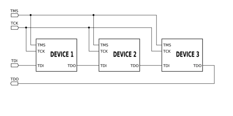
Joint Test Action Group (JTAG) is the common name used for a debugging, programming, and testing interface typically found on microcontrollers, ASICs, and FPGAs. It enables all components with this interface to be tested, programmed, and/or debugged using a single connector on a PC board which can daisy chain them together.
Processors often use JTAG to provide access to their debug/emulation functions and all FPGAs and CPLDs use JTAG to provide access to their programming functions.
JTAG implements standards for on-chip instrumentation in electronic design automation (EDA) as a complementary tool to digital simulation. It specifies the use of a dedicated debug port implementing a serial communications interface for low-overhead access without requiring direct external access to the system address and data buses.
The interface connects to an on-chip test access port (TAP) that implements a stateful protocol to access a set of test registers that present chip logic levels and device capabilities of various parts.
The JTAG standards have been extended by many semiconductor chip manufacturers with specialized variants to provide vendor-specific features.
The debug and programming tools commonly associated with JTAG only make use of one aspect of the underlying technology – the four-wire JTAG communications protocol.
JTAG is the name of the group that defined the IEEE 1149.1 standard. This standard defines the Test Access Port (TAP) controller logic used in processors with JTAG interfaces.
Required below pins –
TMS -Test Mode Select
TCK – Test Clock Input
TDI – Test Data Input
TDO – Test Data Output
TRST – Test Reset (optional)
- TMS – selects the device under test
- TCK – clocks data into TDI
- TDI – the test or programming data input, cascaded through all JTAG compliant devices in the system
- TDO – the resulting output
- TRST – Test reset
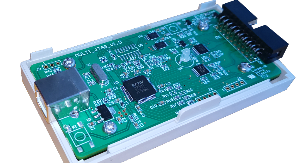
JTAG Connector
There is no standard JTAG connector or pinout, so suppliers are able to define their own. This unique interface enables you to debug the hardware easily in real time (i.e. emulate). It can control directly the clock cycles provided to the micro controller through software. Therefore you can put hardware breakpoints in your code execution. You can start, pause, stop the execution of the code in the hardware as you want. For simplicity, one may assume the following hardware.
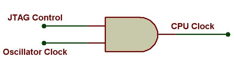
Whenever JTAG control is set to ‘1’, oscillator clock will be connected to CPU, else CPU will not receive clock and cannot execute any instruction. This way, you can control the execution of instructions in hardware.
For programming the CPLDs/FPGAs, JTAG uses parallel port of the computer. However, you can program your micro controllers through USB port.
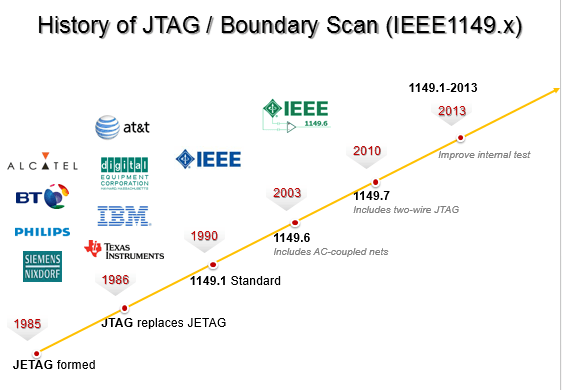
JTAG is a common hardware interface that provides your computer with a way to communicate directly with the chips on a board. It was originally developed by a consortium, the Joint (European) Test Access Group, in the mid-80s to address the increasing difficulty of testing printed circuit boards (PCBs).
JTAG has been in widespread use ever since it was included in the Intel 80486 processor in 1990 and codified as IEEE 1491 that same year. Today JTAG is used for debugging, programming and testing on virtually ALL embedded devices.
Boundary Scanning
With the invention of integrated circuits came the need to test physical interconnects. That is: test whether “Point A” on a circuit board correctly connects to “Point C”. As industry drove toward higher density interconnects and finer pitch (i.e. smaller) components, a standardized way of testing integrated circuits (or “chips”) was needed.
By embedding the test logic within the IC itself and limiting the physical interface to just a few signals, JTAG/boundary-scan presented an elegant solution to testing, debugging, and diagnosing modern electronic systems. Simply stated, boundary Scanning allows you to read and write individual bits, on individual pins, of the individual chips on a board. This ability to read and write 1’s and 0’s directly onto the pins is extremely powerful, but widely misunderstood.
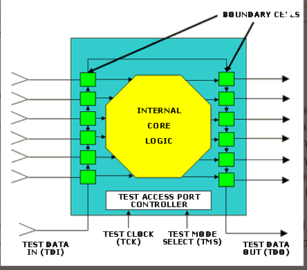
The JTAG interface gives manufacturers a way to test the physical connections between pins on a chip. When electrical engineers talk about using JTAG to “debug” a chip, they are talking about something very different than traditional software debugging. They are talking about making sure pin A on chip A is physically connected to pin B on chip B, and that all those pins are functioning correctly. Since JTAG gives you direct hardware access to a device, it’s also a fantastic tool for security research.
JTAG Fundamentals
Before we go into using JTAG to actually hack something, let’s review the JTAG fundamentals.
4 Pins, Plus 1
The official JTAG standard requires 4 standard pins (or signals), and defines an optional 5th. These signals, and the small bit of silicon logic that connects and controls them, are collectively referred to as the Test Access Port, or TAP controller.
One of the most confusing thing about learning to get hands-on with JTAG is how much partial and disinformation there is about it. Manufacturers’ websites tell you the “theory” of how it works, but leave you longing for more information about “how to get started”. To further confuse things there are other factors:
- Buzzword: It is a infosec buzzword, everyone talks about it but few really share actionable info
- Loaded Word: JTAG has come to mean many things to many people. For example, in the gamer community “JTAG” means a hardware modification for a console that allows playing pirated games or loading homebrew content (i.e. “a jtagged XBox”). This makes it difficult to search for useful information.
- Vernacular Overlap: As mentioned above, when an Electrical Engineer says “debug” he means: “Are the pins in the right place? Is there enough power? Is the logic of the circuit correct?” When a Software Engineer says “debug” he thinks of GDB or WinDBG. JTAG is designed for the former, not the latter.
- Misunderstanding: As software developers the closest similarity to JTAG is maybe Kernel debugging via a debug cable (USB, Parallel, or Serial). But this is a dangerous comparison, because even on the “debugee” (in that scenario) there is software code executing on the remote system handling the translation of commands arriving on the debug cable. The JTAG state machine implemented entirely in hardware on the target.
What JTAG IS: The Five Required JTAG Pins (or “Signals”)
Here is what JTAG is. In it’s most fundamental. The JTAG specification 1149.1 requires these five signals:
- TCK: Test Clock
- The drummer, or metronome that dictates the speed of the TAP controller. Voltage on this pin simply pulses up and down in a rhythmic, steady beat. On every “beat” of the clock, the TAP controller takes a single action. The actual clock speed is not specified in the JTAG standard. The TAP controller accepts its speed from the outside device controlling JTAG.
- TMS: Test Mode Select
- Voltages on the Mode Select pin control what action JTAG takes. By manipulating the voltage on this pin, you tell JTAG what you want it to do.
- TDI: Test Data-In
- The pin that feeds data into the chip. The JTAG standard does not define protocols for communication over this pin. That is left up to the manufacturer. As far as JTAG is concerned, this pin is simply an ingress method for 1s and 0s to get into the chip. What the chip does with them is irrelevant to JTAG.
- TDO: Test Data-Out
- The pin for data coming out of the chip. Like the Data-In pin, communication protocols are not defined by JTAG.
- TRST: Test Reset (Optional)
- This optional signal is used to reset JTAG to a known good state, we’ll explain why this is optional in a few paragraphs.
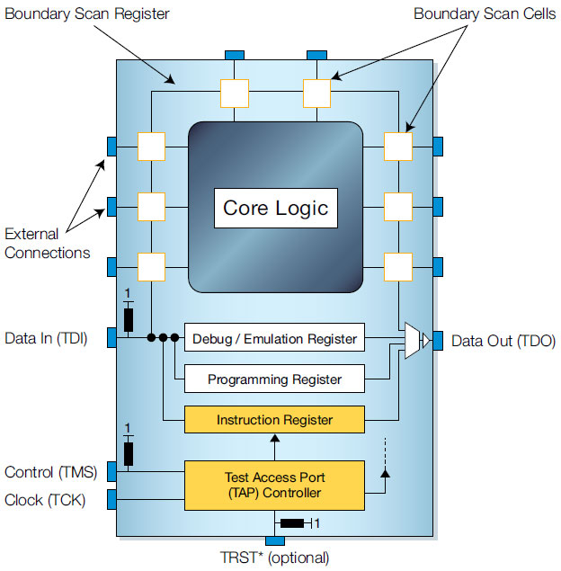
There are two types of registers associated with boundary scan. Each compliant device has one instruction register and two or more data registers.
Instruction Register – the instruction register holds the current instruction. Its content is used by the TAP controller to decide what to do with signals that are received. Most commonly, the content of the instruction register will define to which of the data registers signals should be passed.
Data Registers – there are three primary data registers, the Boundary Scan Register (BSR), the BYPASS register and the IDCODES register. Other data registers may be present, but they are not required as part of the JTAG standard.
- BSR – this is the main testing data register. It is used to move data to and from the I/O pins of a device.
- BYPASS – this is a single-bit register that passes information from TDI to TDO. It allows other devices in a circuit to be tested with minimal overhead.
- IDCODES – this register contains the ID code and revision number for the device. This information allows the device to be linked to its Boundary Scan Description Language (BSDL) file. The file contains details of the Boundary Scan configuration for the device.
How JTAG / Boundary Scan is Used to Test a Board
Boundary scan cells (see above) can operate in two modes. In their functional mode they have no effect on the operation of the device – this is the mode in which they operate when the board is running normally. In their test mode they disconnect the functional core of the device from the pins. By putting boundary scan cells into test mode they can be used to control the values being driven from an enabled device onto a net and also be used to monitor the value of that net.
Disconnecting the control of the pins from the functionality of the enabled device makes boundary scan test development significantly easier than traditional functional test as no device configuration or booting is required to use the pins. By providing a mechanism to control and monitor all the enabled signals on a device from a four-pin TAP, JTAG significantly reduces the physical access required to test a board.
There are two main ways that this boundary scan capability can be used to test a board. The first way, connection testing (see next section) gives good test coverage, particularly for short circuit faults. It is based purely on the JTAG device capabilities, the connections and nets on the board and – in the case of XJTAG – the logic functionality on a board. The second way extends this coverage by using the JTAG enabled devices on a board to communicate with non-JTAG peripheral devices such as DDR RAM and flash.
What is a JTAG Connection Test?
A JTAG connection test will check that the connections around the JTAG enabled devices on a board are the same as those specified in the design.

Where two JTAG enabled pins are meant to be connected the test will make sure one pin can be controlled by the other. Where enabled pins are not meant to be connected they are tested for short circuit faults by driving one pin and checking that these values are not read on the other pins.
Missing pull resistors and ‘stuck-at’ faults can also be found by a connection test as well as faults involving logic devices whose behaviour can be described in a truth table.
XJTAG will automatically generate the vectors required to run a connection test based on the netlist of a board and JTAG information for the enabled devices.
What About Devices That are not JTAG Enabled?
While the main devices, such as processors and FPGAs, are normally JTAG enabled, there will be many devices in every design that are not. DDR, SDRAM, SRAM, flash, MDIO controlled Ethernet PHYs, SPI and I2C temperature sensors, real time clocks, ADCs and DACs are just some examples of such devices.
The connection test will still provide excellent coverage for short circuit faults on the nets linking these non-JTAG devices to JTAG enabled devices; however it cannot check for open circuit faults at either the JTAG device or the non-JTAG device.
In order to add this open circuit coverage it is necessary to communicate with the peripheral device from boundary scan on the enabled device. If communication can be verified, there cannot be an open circuit fault. This type of testing can be very simple, for example lighting an LED and asking an operator to verify it has activated, or more complex, for example writing data into the memory array of a RAM and reading it back.
Is it a lot of Work to Create a JTAG Test System?
Using the libraries for standard non-JTAG components provided by XJTAG, you can get a set of tests up and running for your board with no code development. The library files contain models for all types of non-JTAG devices from simple resistors and buffers to complex memory devices such as DDR3. Because boundary scan disconnects the control of the pins on JTAG devices from their functionality the same model can be used irrespective of the JTAG device controlling a peripheral.
Most boards already contain JTAG headers for programming or debug so there are no extra design requirements.
Where do I get information about the JTAG in my devices?
In order to run any boundary scan based testing it is necessary to have some information about the implementation of JTAG on the enabled devices on a board. This information comes from the BSDL (Boundary Scan Description Language) files for these devices. BSDL files must be made available by the silicon vendor for a device to be compliant with IEEE Std. 1149.1.
Is JTAG test just used in production?
Not at all. One of the key benefits to boundary scan testing is that the only test hardware required is a JTAG controller. Other production test technologies such as flying probe, automated optical/X-ray inspection or bed-of-nails all require specialised test equipment that will not be available on an engineer’s bench.
Using boundary scan during board bring-up can remove uncertainties – hardware engineers can test prototype boards for manufacturing defects before system testing, and even before firmware is complete. Test systems developed at this early stage of the product lifecycle can easily be reused, and extended for production.
Test Access Port (TAP) Controller
The TAP controller, a state machine whose transitions are controlled by the TMS signal, controls the behaviour of the JTAG system. Figure 2, below, shows the state-transition diagram.

All states have two exits, so all transitions can be controlled by the single TMS signal sampled on TCK. The two main paths allow for setting or retrieving information from either a data register or the instruction register of the device. The data register operated on (e.g. BSR, IDCODES, BYPASS) depends on the value loaded into the instruction register.
For more detail on each state, refer to the IEEE 1149.1 Standard JTAG document.
Boundary Scan Instructions
The IEEE 1149.1 standard defines a set of instructions that must be available for a device to be considered compliant. These instructions are:
- BYPASS – this instruction causes the TDI and TDO lines to be connected via a single-bit pass-through register (the BYPASS register). This instruction allows the testing of other devices in the JTAG chain without any unnecessary overhead.
- EXTEST – this instruction causes the TDI and TDO to be connected to the Boundary Scan Register (BSR). The device’s pin states are sampled with the ‘capture dr’ JTAG state and new values are shifted into the BSR with the ‘shift dr’ state; these values are then applied to the pins of the device using the ‘update dr’ state.
- SAMPLE/PRELOAD – this instruction causes the TDI and TDO to be connected to the BSR. However, the device is left in its normal functional mode. During this instruction, the BSR can be accessed by a data scan operation to take a sample of the functional data entering and leaving the device. The instruction is also used to preload test data into the BSR prior to loading an EXTEST instruction.
Other commonly available instructions include:
- IDCODE – this instruction causes the TDI and TDO to be connected to the IDCODE register.
- INTEST – this instruction causes the TDI and TDO lines to be connected to the Boundary Scan Register (BSR). While the EXTEST instruction allows the user to set and read pin states, the INTEST instruction relates to the core-logic signals of a device.
Obtaining the IEEE 1149.1 Standard
The IEEE 1149.1 Standard JTAG specification is available directly from IEEE:
JTAG, JTAG Facilities, JTAG Programmer, JTAG connector
Newer ARM Cortex cores closely resemble this debug model, but build on a Debug Access Port (DAP) instead of direct CPU access. In this architecture (named CoreSight Technology), core and JTAG module is completely independent.
They are also decoupled from JTAG so they can be hosted over ARM’s two-wire SWD interface (see below) instead of just the six-wire JTAG interface. (ARM takes the four standard JTAG signals and adds the optional TRST, plus the RTCK signal used for adaptive clocking.)
The CoreSight JTAG-DP is asynchronous to the core clocks, and does not implement RTCK. Also, the newer cores have updated trace support.