1. What Is an FPGA?
An FPGA, or Field-Programmable Gate Array, is an integrated circuit containing configurable digital logic blocks and programmable interconnections.
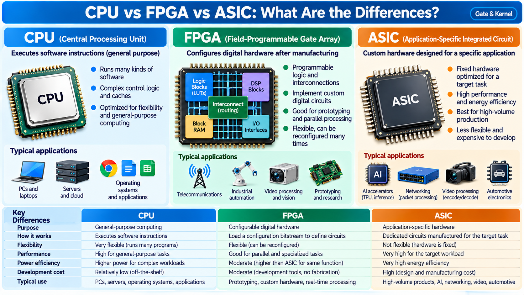
Unlike a conventional CPU, which executes software instructions using a fixed processor architecture, an FPGA allows engineers to configure the digital hardware itself.
FPGAs are widely used in telecommunications, industrial automation, aerospace, robotics, scientific instruments, video processing, and hardware development.
For example, an FPGA can implement a custom communication controller, digital signal processor, hardware accelerator, or even a complete CPU.
The main advantage of an FPGA is hardware flexibility.
Engineers can create digital circuits, test them, and modify their configuration without manufacturing a new semiconductor chip.
However, FPGAs have limitations involving cost, power consumption, maximum performance, and available hardware resources.
Understanding how FPGAs work helps explain the differences between software execution, configurable digital hardware, and custom integrated circuits.
2. What Does FPGA Stand For?
FPGA stands for Field-Programmable Gate Array.
The word field means that the device can be configured after manufacturing, including after it has been installed in an electronic system.
Programmable means that configuration data determines how the device’s logic resources and interconnections behave.
Gate Array refers to its origins as an array of configurable digital logic resources.
Unlike a CPU program, which changes the instructions executed by an existing processor, FPGA configuration determines the digital circuit implemented within the available hardware.
For example, the same FPGA may be configured to implement a UART controller in one project and a digital filter in another.
Many FPGAs support repeated reconfiguration, making them useful for development, prototyping, and applications requiring hardware changes.
3. What Is Inside an FPGA?
A typical FPGA contains several kinds of hardware resources.
Configurable Logic Blocks, or CLBs, provide programmable digital logic. The terminology varies among manufacturers.
Look-Up Tables, or LUTs, implement combinational logic functions.
Flip-flops and registers store binary information.
Programmable interconnections connect logic blocks and other resources.
Block RAM provides dedicated on-chip memory.
DSP blocks accelerate arithmetic operations such as multiplication and accumulation.
Clock management resources distribute and control timing signals.
Input/output blocks connect the FPGA to external electronic devices.
Many modern FPGAs also contain high-speed transceivers, memory interfaces, and specialized hardware blocks.
Some devices integrate hard CPU cores alongside programmable logic.
The exact architecture depends on the FPGA family and manufacturer.
4. How Does an FPGA Work?
An FPGA works by loading configuration data that defines how its programmable hardware resources are connected and used.
For example, suppose an engineer wants to create a digital counter.
The engineer describes the required logic using a hardware description language such as Verilog or VHDL.
Development tools synthesize the design and map it onto the FPGA’s available logic blocks, registers, and interconnections.
The tools then generate a configuration file, commonly called a bitstream.
When the bitstream is loaded, the FPGA’s programmable resources are configured to implement the counter circuit.
The counter can then operate as digital hardware.
Unlike a CPU executing a software loop, the FPGA can implement counting logic directly through configured circuits.
Several independent counters can operate concurrently because they are implemented as separate hardware structures.
This is one of the fundamental advantages of FPGA technology.
5. What Is a Look-Up Table (LUT)?
A Look-Up Table, or LUT, is a basic component of FPGA programmable logic.
A LUT can implement a Boolean function by storing the output values corresponding to possible input combinations.
For example, a four-input LUT can represent a Boolean function with four input variables.
There are 16 possible input combinations, so a conventional four-input LUT can store 16 output values for one Boolean function.
By programming those values, the LUT can implement functions such as AND, OR, XOR, or more complex combinational logic.
Modern FPGAs commonly use LUT structures that support several inputs, although the exact size and organization vary.
Multiple LUTs can be connected to implement larger circuits.
LUTs do not normally execute instructions like a CPU.
Instead, they implement logic functions through configured hardware.
6. What Are FPGA Flip-Flops and Registers?
Flip-flops are digital storage elements that retain binary information.
In synchronous FPGA designs, flip-flops commonly update their stored values on selected clock edges.
For example, a register containing eight flip-flops can store an eight-bit value.
Registers are used in counters, state machines, pipelines, communication controllers, and many other digital circuits.
A counter may increase its stored value on each clock edge.
A state machine may change its current state according to inputs and control conditions.
Registers also allow complex FPGA designs to be divided into pipeline stages.
This makes timing easier to manage and can increase throughput.
LUTs implement combinational logic, while flip-flops provide the state required for sequential digital systems.
Together, they form the foundation of many FPGA circuits.
7. What Are FPGA Programmable Interconnections?
Programmable interconnections allow FPGA resources to be connected into different digital circuits.
An FPGA contains routing wires, switching structures, and connection resources.
Configuration data determines which connections are enabled.
For example, the output of one LUT may be connected to a register or another logic block.
Other connections may link memory blocks, DSP units, and external interfaces.
This routing flexibility allows one FPGA to implement many different hardware designs.
However, programmable routing introduces electrical delay and consumes chip area.
This is one reason an FPGA implementation may have lower maximum performance or higher power consumption than a custom ASIC implementing the same function.
The flexibility is valuable, but it has a physical cost.
8. What Is the Difference Between an FPGA and a CPU?
A CPU executes machine instructions using a processor architecture that is largely fixed after manufacturing.
For example, a CPU can run a program that adds two numbers, processes a network packet, or controls a device.
Changing the software changes what the processor does, but it does not fundamentally replace the CPU’s instruction execution hardware.
An FPGA works differently.
Its programmable resources can be configured to create the digital circuits required by an application.
For example, an FPGA can implement a custom arithmetic pipeline or communication controller.
Multiple operations may execute simultaneously using independent hardware circuits.
However, an FPGA is not automatically faster than a CPU.
A CPU often performs better for tasks involving complex software, unpredictable branches, and general-purpose processing.
An FPGA is attractive when an application benefits from custom hardware, deterministic timing, specialized interfaces, or highly pipelined computation.
The central difference is that a CPU executes software instructions, while an FPGA configures hardware circuits.
9. What Is the Difference Between an FPGA and an ASIC?
An ASIC, or Application-Specific Integrated Circuit, is a chip designed for a particular application or class of functions.
Its main transistor-level circuit structure is established during manufacturing.
An FPGA contains configurable logic and routing resources that can be programmed after manufacturing.
For example, engineers may implement a video-processing circuit on an FPGA during development.
They can modify the design, test different architectures, and correct hardware logic errors without producing a new silicon die.
Once the design becomes stable, a custom ASIC may provide better performance, lower power consumption, or lower unit cost at sufficient production volume.
However, ASIC development requires significant engineering investment and manufacturing expense.
An FPGA generally has lower initial development costs and provides greater flexibility.
The choice depends on performance requirements, production volume, development time, and the need for future hardware changes.
10. FPGA vs. CPU vs. ASIC: Which Is Better?
CPU, FPGA, and ASIC technologies have different strengths.
A CPU provides the greatest flexibility for general-purpose software execution. It is appropriate for operating systems, applications, complex control logic, and workloads requiring frequent software changes.
An FPGA provides configurable digital hardware. It is useful for prototyping, specialized interfaces, real-time processing, and applications that benefit from hardware parallelism.
An ASIC provides hardware optimized for a particular application. It may achieve high performance and energy efficiency when the workload is stable and justifies custom manufacturing.
For example, a CPU can execute software that processes incoming network packets.
An FPGA can implement a configurable hardware packet-processing pipeline.
An ASIC can implement a highly optimized packet-processing architecture for a commercial network switch.
The best approach depends on the system requirements.
No single technology is universally superior.
11. Why Are FPGAs Good at Parallel Processing?
FPGAs can implement multiple independent hardware circuits that operate concurrently.
For example, an engineer can configure an FPGA with several arithmetic units.
Each unit can process a different data stream.
Unlike a conventional CPU program that schedules operations through instructions, these circuits can operate simultaneously as dedicated hardware.
FPGAs can also implement pipelines.
A pipeline divides a computation into stages, with registers storing intermediate results.
Once the pipeline is filled, different stages can process different data items during the same clock cycle.
This can provide high throughput for suitable algorithms.
However, FPGA performance depends on available logic resources, memory bandwidth, clock frequency, routing delay, and circuit architecture.
Parallelism must be explicitly designed and mapped into the available hardware.
12. Can an FPGA Run a CPU?
Yes. An FPGA can implement a processor using its configurable logic resources.
Such a processor is commonly called a soft-core CPU.
For example, engineers can implement RISC-V processor cores inside an FPGA.
The FPGA configuration defines the processor’s registers, arithmetic units, instruction decoding, and control logic.
The resulting processor can execute software compatible with its implemented instruction set.
However, soft-core processors generally have different performance, area, and power characteristics from dedicated hard CPU cores.
Some FPGA devices also integrate hard processor cores manufactured directly into the silicon.
These devices are often called SoC FPGAs.
Combining CPU execution with programmable logic is useful for embedded systems, custom interfaces, and hardware acceleration.
13. What Programming Languages Are Used for FPGA Development?
FPGA engineers commonly use hardware description languages such as Verilog, SystemVerilog, and VHDL.
These languages describe digital hardware behavior and structure.
For example, a Verilog design may describe a counter, finite state machine, arithmetic unit, or communication controller.
The source code is processed by synthesis and implementation tools.
The resulting hardware configuration is loaded into the FPGA.
Although Verilog resembles a programming language, it describes circuits rather than ordinary sequential software execution.
Modern FPGA development may also use High-Level Synthesis, or HLS.
HLS tools can translate supported descriptions written in languages such as C or C++ into hardware implementations.
However, generating efficient hardware still requires an understanding of parallelism, timing, memory, and digital architecture.
14. How Is an FPGA Programmed?
The FPGA development process normally begins with a hardware design.
Engineers write RTL or use another supported design method.
Simulation is used to check the expected behavior.
Synthesis converts the design into logic structures.
Implementation tools map the design onto the FPGA’s logic blocks, registers, memory, and routing resources.
Timing analysis checks whether the implemented circuit meets its clock and timing requirements.
The tools then generate a configuration bitstream.
The bitstream is loaded into the device through a supported programming interface.
Many SRAM-based FPGAs load their configuration after power-up, often from external nonvolatile memory.
Other FPGA technologies use nonvolatile configuration storage.
The exact programming process depends on the FPGA architecture.
15. What Is FPGA Timing Analysis?
Timing analysis determines whether signals can propagate through a digital circuit within the required time limits.
For example, a synchronous circuit may require data to reach a register before the next active clock edge.
If the signal arrives too late, the register may capture an incorrect value or the circuit may behave unreliably.
FPGA implementation tools analyze delays associated with logic blocks, routing, and registers.
Engineers specify clock frequencies and other timing constraints.
The tools evaluate whether the implemented design satisfies those constraints.
A design can be logically correct in simulation but fail timing requirements on real hardware.
Therefore, timing analysis is an essential part of FPGA development.
Clock-domain crossings and asynchronous inputs also require careful design.
16. What Is FPGA Block RAM?
Block RAM, commonly called BRAM, is dedicated memory integrated into many FPGA devices.
Unlike ordinary LUT-based logic, block RAM provides specialized storage resources.
It can be used for data buffers, lookup tables, small memories, and other storage functions.
For example, a digital signal processing pipeline may use block RAM to store intermediate data.
A soft-core CPU may use block RAM for instruction or data memory.
The capacity and configuration options depend on the FPGA family.
Some devices also contain larger embedded memory blocks or support external DDR memory interfaces.
Memory architecture is important because an FPGA design can become limited by memory capacity or bandwidth even when enough logic resources are available.
17. What Are DSP Blocks in an FPGA?
Many FPGAs include dedicated Digital Signal Processing blocks.
DSP blocks commonly support operations such as multiplication, addition, accumulation, and other arithmetic functions.
These operations are important in digital filters, communication systems, image processing, and numerical acceleration.
For example, a digital filter may require many multiply-accumulate operations.
Using dedicated DSP hardware can be more efficient than implementing every multiplication entirely with general-purpose LUTs.
However, DSP block capabilities vary across FPGA families.
Some devices support different operand widths, arithmetic modes, and pipeline configurations.
An efficient FPGA design uses the available DSP resources when appropriate.
18. Where Are FPGAs Used?
FPGAs are widely used in applications requiring configurable or specialized digital hardware.
In telecommunications, they implement high-speed data processing, protocol interfaces, and signal-processing functions.
In industrial automation, they support deterministic control, custom interfaces, and real-time data processing.
In aerospace and scientific instruments, they can implement specialized digital systems.
In video processing, FPGAs can support image pipelines and low-latency transformations.
In networking, they are used for packet processing and protocol development.
In semiconductor engineering, FPGAs are used to prototype digital circuits before ASIC manufacturing.
FPGAs are also valuable in education because students can implement real hardware designs without fabricating custom semiconductor chips.
19. What Are the Advantages of an FPGA?
The main advantage of an FPGA is hardware reconfigurability.
Engineers can modify the implemented digital circuit without manufacturing a new chip.
This makes FPGAs useful for research, prototyping, and products with changing requirements.
FPGAs also support custom hardware parallelism.
Multiple independent circuits can operate concurrently.
Dedicated pipelines can provide predictable throughput and low latency for suitable applications.
FPGAs can also implement specialized interfaces that may not be available on ordinary processors.
Another advantage is reduced initial manufacturing investment compared with custom ASIC development.
These features make FPGAs attractive when flexibility and hardware customization are important.
20. What Are the Disadvantages of an FPGA?
FPGAs also have limitations.
Their programmable logic and routing resources consume silicon area and introduce additional electrical overhead.
For the same function and comparable semiconductor technology, a custom ASIC can often provide better power efficiency, performance, or silicon area.
High-performance FPGAs may also be expensive.
FPGA development requires knowledge of digital logic, timing constraints, clock domains, and hardware verification.
Debugging hardware behavior can be more difficult than debugging ordinary software.
Available LUTs, registers, block RAM, DSP units, and routing resources also limit the size of a design.
Therefore, FPGA flexibility comes with trade-offs in cost, development complexity, and hardware efficiency.
21. How Do You Choose an FPGA?
Choosing an FPGA begins with identifying the required hardware functions.
Estimate how many logic resources, registers, memory blocks, and DSP units the design will need.
Review clock frequency and timing requirements.
Check the number and type of external interfaces.
For example, a design may require GPIO, UART, SPI, high-speed serial transceivers, or DDR memory support.
Power consumption and thermal requirements are also important.
Development tools, documentation, board availability, and licensing costs should be considered.
For beginners, a development board with accessible GPIO, LEDs, buttons, and a straightforward programming interface is often sufficient.
For advanced applications, memory bandwidth, high-speed communication, and specialized hardware blocks may be decisive.
The best FPGA is the one that provides the required resources with an acceptable cost and development environment.
22. A Simple FPGA Project: Building a Counter
A digital counter is an excellent first FPGA project.
The design contains a register that stores the current count value.
On each active clock edge, the counter increases its value according to the circuit logic.
The count can be connected to LEDs or another output interface.
The engineer writes the design using Verilog or VHDL.
Simulation verifies that the counter behaves correctly.
After synthesis and implementation, a bitstream is loaded into the FPGA.
The physical FPGA then executes the counter logic as configured hardware.
The project demonstrates several important concepts, including registers, clock signals, combinational logic, simulation, and hardware implementation.
More advanced projects can include UART communication, PWM generation, memory interfaces, and simple RISC-V processors.
23. Common Misunderstandings About FPGAs
One common misunderstanding is that an FPGA is simply a CPU that can be reprogrammed.
In reality, an FPGA configures digital hardware resources, while a CPU normally executes software using an existing processor architecture.
Another misconception is that FPGA programming works exactly like software programming.
Hardware description languages describe circuits and concurrent behavior, not merely sequential instructions.
Some people assume that FPGAs are always faster than CPUs.
An FPGA may provide advantages for specialized pipelines and custom interfaces, but general-purpose software can run more efficiently on a CPU.
Another misunderstanding is that FPGA circuits can be changed without limitations.
Every FPGA has finite logic, memory, routing, and timing resources.
It is also incorrect to assume that FPGA and ASIC development are completely unrelated.
Both involve digital logic design, verification, synthesis, and timing considerations, although their physical implementations differ.
24. Conclusion: FPGA vs CPU vs ASIC
An FPGA is an integrated circuit containing configurable digital logic and programmable interconnections.
It allows engineers to implement custom digital hardware after the semiconductor chip has been manufactured.
A CPU executes software instructions using a processor architecture.
An FPGA configures hardware circuits that can perform specialized operations concurrently.
An ASIC implements application-specific circuitry manufactured for a particular purpose.
CPUs offer flexibility for general-purpose software.
FPGAs provide hardware reconfigurability and custom digital processing.
ASICs can deliver highly optimized performance and energy efficiency for stable, high-volume applications.
However, every technology involves trade-offs involving development cost, performance, power consumption, flexibility, and production volume.
The most important principle is simple: a CPU runs software, an FPGA configures hardware, and an ASIC implements specialized hardware in manufactured silicon.
Understanding these differences provides a foundation for learning digital logic, Verilog, RISC-V processors, embedded systems, hardware acceleration, and custom chip design.