1. What Is a Semiconductor Die?
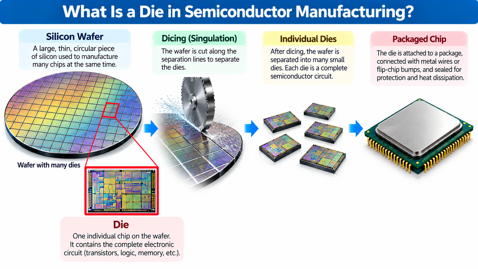
A semiconductor die is an individual piece of semiconductor material containing a fabricated electronic circuit or device.
In modern chip manufacturing, many integrated circuits are produced simultaneously on a large semiconductor wafer.
Each individual circuit area is called a die, and after fabrication, the wafer is separated into individual dies through a process known as dicing or singulation.
The semiconductor die contains the actual electronic circuitry responsible for performing the chip’s functions.
Depending on the design, a die may contain transistors, logic gates, memory cells, arithmetic units, communication circuits, analog components, and electrical interconnections.
For example, a CPU die may contain processor cores, cache memory, memory interfaces, and other functional blocks.
A memory die contains arrays of memory cells and the supporting circuits required to store and retrieve information.
A die is usually much smaller than the wafer from which it was manufactured.
It is commonly rectangular or square, although specialized semiconductor devices can have other shapes.
After being separated from the wafer, the die usually undergoes additional assembly and packaging operations.
The package provides electrical connections, mechanical protection, and a suitable path for heat transfer.
The difference between a semiconductor die and a packaged chip is important.
The die contains the manufactured electronic circuit, while the package allows that circuit to be connected to a larger electronic system.
Understanding what a die is provides an essential foundation for studying silicon wafers, chip fabrication, semiconductor yield, packaging technology, CPUs, GPUs, memory devices, and modern chiplet architectures.
2. What Does the Word Die Mean in Electronics?
In semiconductor manufacturing, the word die refers to an individual semiconductor circuit area, especially one intended to be separated from a wafer.
The word is used throughout the chip design, fabrication, testing, and packaging industries.
For example, engineers may discuss die size, die area, die yield, die temperature, or die placement.
The plural form is commonly written as dies or dice. Both are used in semiconductor engineering.
A die may be described while it is still part of the wafer. After separation, it becomes an individual physical piece of semiconductor material.
A bare die is a die that has not been enclosed in a conventional protective package.
A known good die, or KGD, is a die that has passed an appropriate set of tests or screening requirements intended to establish its suitability for further assembly.
These terms are especially important in advanced packaging, where multiple dies may be assembled into one package.
The term die should not be confused with the word chip in every context.
In everyday language, people often call a finished packaged semiconductor device a chip, while engineers may use chip to refer to the bare semiconductor die.
The exact meaning depends on the context.
3. What Is the Difference Between a Wafer and a Die?
A wafer is a thin, circular semiconductor substrate used to manufacture many electronic circuits simultaneously.
A die is one individual circuit area on that wafer.
For example, a 300-millimeter silicon wafer may contain hundreds of copies of a processor design.
Each copy occupies a particular rectangular region of the wafer.
During fabrication, the wafer remains largely intact while semiconductor devices and interconnections are constructed across its surface.
After fabrication and appropriate testing, the wafer is separated into individual dies.
Therefore, a wafer is the larger manufacturing substrate, while a die is the smaller semiconductor product obtained from it.
The distinction is similar to manufacturing many individual components from one larger sheet of material, although semiconductor processing is far more complex.
The wafer enables efficient parallel manufacturing because many circuit copies can undergo the same processing operations.
The die becomes the functional unit used in subsequent testing, packaging, and electronic system assembly.
4. What Is the Difference Between a Die and a Chip?
The terms die and chip are closely related, but they are not always identical.
A semiconductor die is the physical piece of processed semiconductor material containing the electronic circuit.
The word chip is more flexible.
In semiconductor engineering, chip may refer to the die itself.
In consumer electronics, chip often describes the completed packaged device.
For example, when someone purchases a microcontroller, the component usually comes in a protective package with electrical terminals.
The actual silicon die is located inside that package.
Similarly, a desktop processor appears to be a small packaged component, but its circuitry is contained in one or more semiconductor dies.
Modern processors may combine multiple dies in a single package.
Therefore, it is useful to distinguish among the semiconductor die, the package, and the finished chip product.
A die is not necessarily the same thing as the entire processor package.
5. What Is the Difference Between a Die and an Integrated Circuit?
An integrated circuit, or IC, is an electronic circuit in which multiple components are fabricated and interconnected on or within semiconductor material.
A die is the physical semiconductor piece containing the fabricated circuit.
The distinction is between the electronic function and its physical implementation.
For example, a processor integrated circuit may contain billions of transistors connected to execute machine instructions.
The silicon die physically contains those transistors and interconnections.
Once the die is packaged, the resulting device can be mounted on a circuit board or integrated into another electronic system.
An integrated circuit is therefore commonly implemented as a semiconductor die, but the two terms emphasize different aspects of the product.
It is also important to recognize that some semiconductor dies contain devices that are not conventional large-scale digital integrated circuits.
For example, a die may contain a power semiconductor device, optical sensor, or specialized analog structure.
The concept of a semiconductor die is broader than a particular type of processor.
6. Why Are Semiconductor Dies Usually Rectangular?
Most semiconductor dies are rectangular or square because integrated circuit layouts and manufacturing processes are generally organized around rectangular design regions.
Digital chip design uses structured arrangements of cells, memory arrays, routing channels, and other functional blocks.
These structures are commonly organized within rectangular physical boundaries.
During wafer fabrication, many die layouts are repeated across the circular wafer surface.
Narrow separation regions are left between adjacent dies.
After fabrication, the wafer can be cut along these separation regions to produce individual rectangular pieces.
Rectangular dies also provide practical advantages for placement, packaging, and electrical connection design.
However, rectangular geometry is not a strict physical requirement for every semiconductor device.
Certain sensors, optical components, and specialized devices may use different geometries.
For mainstream processors and memory devices, rectangular or square die shapes are the most common.
7. What Is Inside a Semiconductor Die?
The internal structure of a semiconductor die depends on the function of the device.
A digital processor die contains many transistor-based circuits.
These may include arithmetic units, registers, instruction processing logic, caches, memory controllers, and communication interfaces.
A memory die contains large arrays of storage cells, address decoders, sense amplifiers, and control circuits.
An analog IC die may contain amplifiers, references, filters, resistors, capacitors, and other components.
A power semiconductor die may contain structures optimized for controlling substantial electrical currents and voltages.
Modern semiconductor dies also contain electrical interconnections.
Multiple conductive layers connect the devices into functioning circuits.
These layers are separated by insulating materials and connected through vertical conductive structures called vias.
The result is a complex three-dimensional electronic structure.
The silicon die does not merely support components placed on top of it.
Much of the device structure is manufactured in or near the semiconductor substrate, with additional layers built above it.
8. How Are Transistors Formed Inside a Die?
Modern digital semiconductor dies rely heavily on transistors.
A transistor is a semiconductor device that controls electrical behavior, often functioning as an electronic switch.
In a simplified MOSFET, a gate voltage influences the conductivity of a channel between the source and drain.
By arranging MOSFETs into suitable circuits, engineers create logic gates and storage elements.
Semiconductor manufacturing uses repeated operations to form these structures.
Important processes include deposition, photolithography, etching, doping, annealing, and polishing.
The exact process depends on the transistor technology.
Conventional planar MOSFETs use relatively flat channel structures.
FinFETs use raised fin-shaped semiconductor channels.
Gate-all-around transistors use structures in which the gate surrounds the channel more completely.
After transistor formation, electrical contacts and metal interconnections are added.
This produces the electronic circuits contained in each die.
9. How Is a Die Designed Before Manufacturing?
A semiconductor die begins as an electronic design.
Engineers first define the functions the chip must perform.
For a processor, these requirements may include instruction execution, cache capacity, memory interfaces, power consumption, and target performance.
Digital hardware designers commonly use hardware description languages such as Verilog and SystemVerilog.
The design may be represented at the Register Transfer Level, or RTL.
RTL describes how digital information moves between registers and how logical operations are performed.
Electronic design automation tools convert the RTL into a gate-level implementation.
Physical design tools then determine how the required cells and larger functional blocks should be placed and interconnected.
The resulting physical layout defines the circuitry to be manufactured.
The layout must satisfy manufacturing rules, timing requirements, power constraints, and other specifications.
The final die dimensions are influenced by the area required for circuitry, memory, interfaces, routing, and manufacturing-related structures.
Therefore, die size is an engineering result rather than an arbitrary number selected after fabrication.
10. What Is Die Size?
Die size describes the physical dimensions of a semiconductor die.
It is commonly expressed using length and width, or as a total area measured in square millimeters.
For example, a rectangular die measuring 10 millimeters by 12 millimeters has an area of 120 square millimeters.
A larger die generally occupies more wafer area.
However, die size does not directly determine computing performance.
A large processor may contain extensive cache memory and many execution units.
A smaller processor may provide better performance for certain workloads because of its architecture, operating frequency, or other characteristics.
Die size affects manufacturing economics because fewer large dies generally fit on one wafer.
It can also influence defect exposure, packaging requirements, thermal behavior, and interconnection design.
Chip designers therefore balance performance, functionality, power consumption, and area.
This relationship is often described using the abbreviation PPA, meaning Power, Performance, and Area.
11. How Is Die Area Calculated?
For a rectangular semiconductor die, the basic area calculation is straightforward.
Die Area = Length × Width
For example, consider a die measuring 8 millimeters by 10 millimeters.
Its area is 80 square millimeters.
A die measuring 20 millimeters by 20 millimeters has an area of 400 square millimeters.
Although the second die is only twice as wide and twice as tall, it occupies five times the area of the first die.
This illustrates why increasing die dimensions can significantly influence manufacturing cost.
However, die area alone does not indicate how many transistors are present.
Transistor density depends on the manufacturing process, circuit architecture, memory structures, and physical design.
Two dies with the same area may contain very different circuits and transistor counts.
12. How Many Dies Fit on a Silicon Wafer?
The number of dies that fit on a wafer depends on wafer diameter, die dimensions, and layout requirements.
A larger wafer provides more surface area.
A smaller die generally allows more copies to be manufactured on the same wafer.
For example, a 300-millimeter wafer has a larger surface area than a 200-millimeter wafer.
If both wafers use the same die design and process, the larger wafer can usually accommodate more complete dies.
However, the calculation is not simply wafer area divided by die area.
A wafer is circular, while most dies are rectangular.
Some areas near the wafer edge cannot accommodate complete rectangular dies.
Manufacturers must also account for separation lanes and other layout constraints.
The resulting number of candidate dies is commonly called gross dies per wafer.
The number of usable dies is usually lower because some devices may fail testing.
13. What Are Gross Dies per Wafer?
Gross dies per wafer refers to the number of candidate die locations that can be placed on a wafer before accounting for manufacturing test failures.
The value depends on wafer diameter, die size, die shape, edge exclusions, and other layout requirements.
For example, reducing die area may allow more candidate dies to fit on the same wafer.
However, the increase is not always proportional because rectangular dies must fit within the circular wafer boundary.
Engineers use mathematical estimates and specialized layout tools to determine die counts.
Simple models are useful for understanding manufacturing economics, but production estimates must account for the actual wafer and die geometry.
Gross dies per wafer is not the same as the number of good dies.
A wafer can contain many candidate dies while only a portion meet the required electrical specifications.
14. What Is a Good Die?
A good die is a semiconductor die that meets the relevant acceptance criteria during testing.
The criteria depend on the product.
For example, a processor die may be tested for functional correctness, memory behavior, voltage characteristics, leakage current, and operating frequency.
A memory die may be tested for storage functionality, timing, and other electrical properties.
Some dies fail because of manufacturing defects.
Others may work correctly but not satisfy the performance or power requirements of a particular product category.
Manufacturers may classify functioning dies according to their measured characteristics.
A die that does not qualify for one product grade may sometimes be suitable for another supported configuration.
However, not every defective die can be reused.
The final determination depends on the chip design, manufacturing process, and test specifications.
15. What Is Die Yield?
Die yield is the proportion of candidate dies that satisfy the relevant manufacturing acceptance criteria.
For example, suppose a wafer contains 200 candidate dies.
If 180 pass testing, the simplified die yield is 90 percent.
Die Yield = Good Dies ÷ Candidate Dies × 100%
Yield is one of the most important economic measures in semiconductor manufacturing.
The wafer fabrication process is expensive, and each defective die represents manufacturing resources that did not produce an acceptable product.
Yield depends on many factors, including defect density, die area, process maturity, manufacturing variations, circuit design, and testing requirements.
A larger die may be more vulnerable to certain types of random manufacturing defects because it occupies more area.
However, the relationship between die size and yield depends on the actual defect model and product architecture.
Some chips include redundant structures or repair mechanisms that improve the number of acceptable devices.
16. Why Do Larger Dies Often Have Lower Yield?
Larger dies occupy more semiconductor area.
If random manufacturing defects occur across a wafer, a larger die has a greater opportunity to intersect one or more defects.
For example, consider two designs manufactured using the same process.
One die occupies 50 square millimeters, while another occupies 400 square millimeters.
Under a simplified random defect model, the larger die has a higher probability of containing a defect.
However, not every physical defect necessarily causes a functional failure.
The effect depends on the defect’s location, size, and interaction with the circuit.
Some designs contain redundant memory blocks or other mechanisms that can tolerate selected defects.
Manufacturing defects are also not always randomly distributed.
They may be clustered or associated with specific processing problems.
Therefore, larger die area is an important yield consideration, but it is not sufficient by itself to calculate actual production yield.
17. What Is a Scribe Lane?
A scribe lane is a narrow separation region between adjacent dies on a semiconductor wafer.
It is also commonly called a dicing street.
The scribe lane provides space for separating the finished wafer into individual dies.
During fabrication, each die contains the circuitry required by the intended product.
The separation regions help establish where cutting or another singulation process can occur.
Scribe lanes may also contain test structures used for process monitoring and electrical measurements.
These structures can provide information about transistor characteristics, interconnect resistance, and other manufacturing parameters.
The scribe lane is not simply unused space.
It can support both manufacturing separation and process evaluation.
Its required dimensions depend on the fabrication and dicing methods.
18. How Is a Wafer Cut into Individual Dies?
The process of separating a wafer into individual dies is called wafer dicing or singulation.
After the wafer has completed appropriate fabrication and testing operations, it is prepared for separation.
The wafer may be mounted onto an adhesive film supported by a frame.
This helps keep the individual dies in place during and after cutting.
A precision dicing system separates the wafer along the designated streets.
Mechanical dicing blades are one established method.
Laser-based techniques and other specialized processes are also used for suitable products.
The method depends on wafer material, thickness, device structure, die size, and packaging requirements.
The cutting operation must avoid damaging the active circuitry.
After separation, the dies can be inspected and selected for assembly.
19. What Is Wafer Dicing Tape?
Dicing tape is an adhesive film used to support wafers during the singulation process.
The wafer is attached to the tape before or during preparation for cutting.
When the wafer is separated into individual dies, the tape helps retain the pieces in their original positions.
This reduces uncontrolled movement and assists later handling.
Some dicing tapes use adhesives whose holding characteristics can be modified through ultraviolet exposure or other controlled processes.
After dicing, suitable equipment can select individual dies from the tape.
The dies are then transferred to packaging or other assembly operations.
Although dicing tape is not part of the final electronic circuit, it plays an important role in semiconductor manufacturing.
It helps manufacturers handle extremely small and delicate devices efficiently.
20. What Happens to Dies After Dicing?
After dicing, individual semiconductor dies must be handled and prepared for assembly.
Automated equipment can identify and pick acceptable dies.
The selection process may use wafer test information or additional inspection results.
The dies are then transferred to an appropriate packaging operation.
A die may be attached to a leadframe, package substrate, or another supporting structure.
Electrical connections are created using methods such as wire bonding or flip-chip bonding.
Additional materials may be applied for mechanical support or protection.
For some advanced devices, multiple dies are assembled into one package.
After assembly, packaged devices undergo further testing.
The goal is to convert the bare die into a usable electronic component that can be connected reliably to an external system.
21. What Is Die Attach?
Die attach is the process of securing a semiconductor die to a supporting structure during assembly.
The supporting structure may be a leadframe, package substrate, or another component.
The attachment method depends on the package design, electrical requirements, and thermal characteristics.
Some devices use adhesive materials.
Others use solder-based attachment or specialized bonding techniques.
For high-power semiconductor devices, the die attach material may also provide an important thermal path.
Poor die attachment can create mechanical reliability problems or interfere with heat transfer.
The process must therefore control alignment, bonding quality, material properties, and other assembly conditions.
Die attach is one of the important stages that converts a separated semiconductor die into a packaged electronic product.
22. What Is Wire Bonding?
Wire bonding connects electrical pads on a semiconductor die to corresponding package connections using very fine conductive wires.
The wires may be made from suitable materials such as copper, gold, or aluminum, depending on the packaging process.
A bonding machine creates the required connections between the die and the package.
Wire bonding has been widely used for many types of semiconductor products.
It can provide an economical and reliable connection method when the device’s electrical and packaging requirements are suitable.
However, wire bonds introduce physical dimensions and electrical characteristics that must be considered.
For very high connection counts or certain high-performance applications, alternative interconnection techniques may be preferable.
Wire bonding remains important in semiconductor assembly even as advanced packaging methods become more common.
23. What Is Flip-Chip Packaging?
Flip-chip packaging is a method in which the active side of the semiconductor die faces toward the package substrate or another connection structure.
Instead of relying primarily on wires around the die perimeter, flip-chip assembly uses bumps or other conductive features to establish connections.
The die is aligned and bonded to corresponding contacts.
This can allow electrical connections to be distributed across much of the die area.
Flip-chip technology is widely used in many high-performance processors and other complex integrated circuits.
It can support high connection density and suitable electrical performance.
However, the assembly process requires precise alignment and careful mechanical design.
Thermal expansion differences, bonding reliability, and package structure must also be considered.
Flip-chip is not necessary for every IC.
Wire bonding and other packaging methods remain useful for many semiconductor devices.
24. What Is the Difference Between a Bare Die and a Packaged IC?
A bare die is a semiconductor piece containing fabricated electronic circuitry without a conventional protective package.
A packaged IC includes one or more dies assembled into a structure that provides external connections and mechanical protection.
For example, a bare processor die may expose delicate surfaces and connection structures that are not suitable for ordinary handling.
The package provides a more practical interface to the outside system.
It may contain a substrate, electrical contacts, protective materials, and thermal management structures.
Some bare dies are used directly in specialized assemblies.
For example, certain multichip modules, sensors, and advanced packaging systems incorporate bare dies into larger structures.
However, most ordinary electronic components sold for circuit board assembly are packaged devices.
The package is therefore an important part of making semiconductor circuitry usable.
25. Why Is Chip Packaging Important?
Packaging serves several functions.
First, it provides electrical connections between the semiconductor die and the external circuit.
Second, it protects delicate semiconductor structures and interconnections.
Third, it provides mechanical support.
Fourth, it helps manage heat generated during operation.
For example, a high-performance processor may use a package substrate and heat spreader to support electrical and thermal requirements.
A small low-power microcontroller may use a simpler plastic package.
Advanced packaging may also connect multiple dies into one system.
The package design affects signal integrity, power delivery, heat dissipation, reliability, and manufacturing cost.
Therefore, packaging is not merely a final cosmetic step.
It is an essential part of semiconductor engineering.
26. Can One Processor Contain Multiple Dies?
Yes. A modern processor package can contain more than one semiconductor die.
For example, a processor may use separate compute dies and I/O dies.
The compute dies may contain CPU cores and associated cache structures.
An I/O die may contain memory controllers, communication interfaces, and other system functions.
These dies communicate through suitable package interconnections.
This architecture is often associated with chiplet-based designs.
However, not every multi-die package uses the same partitioning strategy.
Some products combine computing dies with memory dies.
Others use vertically stacked dies or specialized interposer connections.
A package containing several dies may still be sold as one processor or semiconductor product.
The distinction between die and package is therefore especially important for understanding modern processors.
27. What Is a Chiplet?
A chiplet is a semiconductor die designed to operate as part of a larger multi-die system.
Instead of placing all functions on one monolithic die, engineers may divide the design into several smaller components.
These chiplets are connected through advanced packaging technology.
For example, a processor may contain multiple computing chiplets and a separate interface die.
This approach can provide manufacturing flexibility.
Different chiplets may use different semiconductor process technologies.
For example, compute logic may benefit from a more advanced process, while certain interface functions may be manufactured economically using a mature process.
Chiplets can also make it possible to reuse certain design components across multiple products.
However, they introduce challenges involving communication latency, bandwidth, power consumption, thermal management, and package cost.
Chiplets are not automatically superior to monolithic dies.
Their benefits depend on the complete system design.
28. What Is a Monolithic Die?
A monolithic die is a single semiconductor die containing the relevant integrated circuit functions.
For example, a processor implemented on one die may contain CPU cores, caches, memory controllers, and other components within one continuous piece of silicon.
The functional blocks communicate through on-die interconnections.
A monolithic design can provide certain advantages in communication latency and integration.
However, manufacturing a very large die can present challenges involving yield and cost.
A chiplet architecture divides selected functions across multiple dies.
The trade-off depends on the architecture and manufacturing technology.
Monolithic and chiplet designs are therefore alternative approaches to implementing complex semiconductor systems.
Neither approach is universally best.
29. What Is a Known Good Die?
Known Good Die, or KGD, is a term used for a semiconductor die that has undergone testing or screening intended to establish sufficient confidence in its functionality before further assembly.
KGD is particularly important when multiple dies are combined into one package.
Suppose a package requires four separate semiconductor dies.
If one die is defective, the entire assembled package may fail or require costly rework.
Testing dies before assembly helps reduce this risk.
However, verifying an unpackaged die can be challenging because some operating conditions may be difficult to reproduce before packaging.
The extent and meaning of KGD testing depend on the product and manufacturing process.
It does not guarantee that a die can never fail.
Further assembly and final testing remain important.
KGD is a critical concept in advanced packaging and multichip integration.
30. Why Are Chiplets Important for Semiconductor Yield?
Very large semiconductor dies can be expensive to manufacture because they occupy substantial wafer area and may have lower yield under certain defect conditions.
Dividing a system into smaller dies can sometimes improve the yield of individual components.
For example, several smaller compute chiplets may be manufactured separately instead of using one very large monolithic die.
However, producing smaller dies does not eliminate defects.
The manufacturer must still obtain enough functioning chiplets to assemble the final product.
Additional packaging and interconnection operations also introduce cost and yield considerations.
The economic advantage depends on die size, defect density, process cost, packaging yield, and system architecture.
Chiplets can offer important benefits, but their value must be evaluated across the complete manufacturing process.
31. How Does Die Size Affect Chip Cost?
Die size influences how many devices can be produced from one wafer.
A smaller die generally allows more candidate dies per wafer.
A larger die generally reduces the candidate die count.
If the wafer processing cost remains similar, fewer usable dies can increase the fabrication cost allocated to each chip.
Yield further influences the result.
For example, if a large die has a lower production yield than a smaller die, its effective manufacturing cost per acceptable unit may increase.
However, chip cost also depends on many other factors.
These include process technology, mask costs, packaging, testing, design engineering, production volume, and product specifications.
Some advanced processors use expensive packaging that contributes substantially to total cost.
Therefore, die area is important, but it is not the only factor determining the selling price of a finished chip.
32. Does a Larger Die Mean a Faster Processor?
Not necessarily.
A larger die may contain more processor cores, additional cache memory, or specialized execution units.
These resources can improve performance in workloads that use them effectively.
However, die size alone does not determine processing speed.
For example, a smaller processor with a more efficient architecture may perform better on certain applications.
Clock frequency, instruction execution efficiency, memory latency, cache organization, software behavior, and thermal constraints all influence performance.
A larger die may also require more complex power distribution and cooling.
Likewise, a smaller die manufactured on a newer process may contain a high transistor density.
The best way to evaluate a processor is through its architecture, specifications, and measured performance in relevant workloads.
Die size is useful for understanding physical design and manufacturing economics, not as a universal performance rating.
33. What Is a CPU Die?
A CPU die is a semiconductor die containing processing circuitry designed to execute machine instructions.
A CPU die may contain one or more processor cores.
It may also include cache memory, memory management units, interconnect structures, and other functional blocks.
The exact design depends on the processor architecture.
Some processor packages contain one monolithic CPU die.
Others contain multiple compute chiplets and additional dies.
Modern CPU dies may contain billions of transistors.
These transistors form logic gates, registers, arithmetic units, control circuits, and memory structures.
The processor executes software instructions by coordinating these hardware resources.
A CPU die is therefore the physical semiconductor implementation of the relevant processor circuitry.
34. What Is a GPU Die?
A GPU die is a semiconductor die containing a graphics processing architecture.
GPUs are designed to provide high computational throughput for graphics and suitable parallel workloads.
A GPU die may contain many arithmetic execution resources, register files, cache memory, control logic, and specialized hardware.
Modern GPUs can also contain dedicated units for matrix operations, video processing, and other functions.
The GPU die communicates with memory and other system components through appropriate interfaces.
Some GPU products use one large compute die.
Others use more complex multi-die architectures or advanced memory packaging.
As with CPUs, GPU performance depends on architecture, operating conditions, memory bandwidth, and software utilization rather than die size alone.
35. What Is a Memory Die?
A memory die is a semiconductor die containing circuits designed primarily to store information.
Different memory technologies use different storage structures.
DRAM dies contain arrays of dynamic memory cells and supporting circuits.
NAND flash dies contain nonvolatile memory arrays and supporting control structures.
SRAM is widely used within processors and other integrated circuits, although dedicated SRAM devices also exist.
For example, a DRAM package may contain one or more memory dies, depending on the product design.
A NAND flash package can contain multiple stacked dies to increase storage capacity.
The completed memory device also requires suitable interfaces and control circuitry.
Memory dies illustrate how packaging can combine multiple semiconductor pieces into one compact component.
36. Why Are NAND Flash Dies Often Stacked?
NAND flash memory is widely used in solid-state drives, smartphones, and other storage systems.
Manufacturers may place multiple NAND dies within one package to increase capacity.
This is different from the vertical layering of memory cells inside an individual 3D NAND die.
A 3D NAND die contains multiple vertically arranged memory cell layers manufactured as part of its semiconductor structure.
Multiple complete NAND dies may then be stacked or otherwise assembled within a package.
These are two different levels of integration.
The first involves the internal structure of the memory die.
The second involves packaging several separate dies together.
Both techniques can contribute to higher storage density.
Understanding this distinction helps avoid confusion between 3D NAND cell architecture and stacked-die packaging.
37. What Is Die Stacking?
Die stacking is the process of arranging multiple semiconductor dies vertically within a package or integrated assembly.
This can reduce the physical footprint of the system and provide opportunities for high-density interconnection.
Different technologies can be used to connect stacked dies.
These may include wire bonding, through-silicon vias, hybrid bonding, or other interconnection approaches.
The best method depends on the electrical and mechanical requirements.
Memory devices commonly use stacked-die arrangements.
Advanced computing systems may also use vertical integration to connect logic and memory structures.
However, stacking introduces thermal and manufacturing challenges.
Heat generated by one die may affect neighboring dies.
Testing and assembly yield also become more important.
Die stacking is therefore a sophisticated packaging technique rather than simply placing chips on top of one another.
38. What Is a Through-Silicon Via?
A Through-Silicon Via, commonly abbreviated TSV, is a vertical electrical connection that passes through a silicon die or substrate.
TSVs are used in certain three-dimensional semiconductor integration technologies.
They can connect stacked dies through relatively short vertical paths.
For example, some high-bandwidth memory architectures use TSV-based connections between vertically stacked memory dies.
The technology can provide high interconnection density.
However, manufacturing TSVs requires additional processing and precise alignment.
TSVs also introduce considerations involving mechanical stress, electrical behavior, heat transfer, and reliability.
Not every stacked semiconductor package uses TSVs.
Other packaging and bonding approaches may be more suitable depending on the product.
39. What Is High-Bandwidth Memory (HBM)?
High-Bandwidth Memory, or HBM, is a memory technology that uses vertically stacked DRAM dies and a wide interface to provide high memory bandwidth.
HBM is particularly important in high-performance computing and AI accelerator systems.
Multiple DRAM dies are integrated into a memory stack.
The stack communicates with processing hardware through an appropriate high-density packaging architecture.
TSVs and other advanced interconnections help support vertical communication within the memory stack.
HBM can provide substantial memory bandwidth while supporting different energy and packaging trade-offs from conventional memory modules.
However, it requires sophisticated manufacturing, packaging, and thermal engineering.
HBM demonstrates why understanding the difference between a wafer, die, chiplet, and package is important for modern computer architecture.
A finished accelerator package may contain several kinds of semiconductor dies serving different functions.
40. What Is Die-to-Die Communication?
Die-to-die communication refers to the transfer of information between semiconductor dies within a package or tightly integrated system.
In a monolithic processor, functional blocks communicate through interconnections fabricated on one die.
In a multi-die processor, certain communications must cross physical die boundaries.
These connections require suitable electrical interfaces and packaging structures.
Important considerations include bandwidth, latency, power consumption, signal integrity, and reliability.
Different products use different interconnection technologies.
For example, some advanced packages use interposers, silicon bridges, or other high-density routing structures.
Industry efforts such as Universal Chiplet Interconnect Express, or UCIe, also address standardized die-to-die connectivity.
However, not every chiplet-based processor uses the same interconnect standard.
The communication architecture is an important part of the performance and efficiency of multi-die systems.
41. What Is an Interposer?
An interposer is an intermediate structure used to provide electrical connections between semiconductor dies and other package components.
It can contain fine conductive routing that connects dies positioned close to one another.
Some advanced semiconductor packages use silicon interposers.
These structures can support dense interconnections between processor dies and memory stacks.
Other packages may use organic or alternative interconnection substrates.
The choice depends on electrical performance, cost, size, and manufacturing requirements.
Interposers are particularly useful when large numbers of signals must move between components within one package.
However, they introduce additional fabrication and assembly considerations.
An interposer is not necessarily a processor die.
Its primary function may be to provide interconnections rather than general-purpose computation.
42. How Are Dies Connected to a Package Substrate?
A package substrate provides electrical pathways between semiconductor dies and the outside system.
It may contain multiple conductive routing layers.
A die can be attached using flip-chip bumps or another suitable method.
The substrate then routes power and signals toward package terminals.
For example, a processor package may use an array of contacts on its underside to connect to a motherboard.
The substrate helps distribute connections from the dense die interface to the larger spacing required by the external circuit.
In multi-die packages, the substrate may also support communication between different dies.
The electrical properties of the substrate influence signal integrity and power delivery.
Package substrate design is therefore an important part of semiconductor system engineering.
43. How Does Heat Leave a Semiconductor Die?
A semiconductor die generates heat because electrical energy is dissipated during operation.
In digital circuits, switching activity and leakage contribute to power consumption.
In power devices, conduction and switching losses may generate substantial heat.
The heat must travel through suitable materials toward the external environment.
For a processor, a thermal path may include the silicon die, thermal interface material, heat spreader, heatsink, and surrounding air or cooling liquid.
The package is designed to support this heat transfer.
However, temperature can vary across the die.
Some functional blocks may dissipate more power than others, creating localized hot spots.
Modern processors often include temperature monitoring and power management mechanisms.
These systems help keep the device within supported operating conditions.
Die temperature is therefore an important factor in processor reliability and performance.
44. What Is Die Temperature?
Die temperature refers to the temperature within the semiconductor die, often measured or estimated at particular locations.
A processor may include several thermal sensors distributed across the chip.
Different sensors can report different temperatures because heat generation is not uniform.
For example, a heavily loaded processor core may operate at a higher temperature than another region.
The reported temperature may also differ from the temperature of the package surface or external heatsink.
Semiconductor devices have specified operating temperature limits.
If the device approaches its limits, power management systems may reduce frequency, voltage, or activity.
This can help prevent overheating.
The permitted operating temperature depends on the particular semiconductor product and its specifications.
Die temperature is important in processors, memory devices, power electronics, and other applications where thermal behavior affects performance or reliability.
45. What Is Die Thinning?
Die thinning is a manufacturing process that reduces the thickness of semiconductor material after certain fabrication operations.
For example, the backside of a wafer may be ground or polished to reduce its thickness before dicing or advanced packaging.
Thinner dies may be useful in stacked memory, compact packages, and other specialized assemblies.
Reducing thickness can provide mechanical or integration advantages.
However, thin dies are more fragile and require careful handling.
The process must avoid excessive stress, cracking, or damage.
Different products require different final die thicknesses.
A semiconductor die is not necessarily as thick as the original wafer from which it was manufactured.
Die thinning is especially important in certain advanced packaging and three-dimensional integration technologies.
46. What Is a Defective Die?
A defective die is a semiconductor die that fails one or more required acceptance criteria.
The failure may result from a manufacturing defect, circuit problem, electrical variation, or another condition.
For example, an unintended electrical short may prevent part of the circuit from functioning.
An open connection may interrupt communication between components.
A memory array may contain defective storage cells.
Some defects are detected during wafer testing.
Others may become apparent during packaging, final testing, or reliability screening.
Not every defect necessarily makes the entire die unusable.
Certain designs contain redundancy or support disabling selected functional units.
However, the ability to recover or classify a partially functional die depends on the product architecture.
Manufacturers use testing and yield analysis to determine which dies are suitable for further assembly.
47. What Is Processor Binning?
Binning is the process of classifying manufactured semiconductor devices according to measured characteristics.
Even dies produced from the same design and manufacturing process may exhibit differences in electrical behavior.
For example, some processor dies may operate reliably at a higher frequency under specified voltage and thermal conditions.
Others may meet a lower performance target.
Manufacturers can sort these devices into different product categories.
Some designs also support disabling particular cores, cache regions, or other structures.
This may allow certain dies to be sold in configurations that meet a different set of specifications.
However, the actual binning process depends on the manufacturer and product design.
Binning demonstrates that semiconductor production does not always produce perfectly identical electrical characteristics across every die.
48. How Is a Semiconductor Die Tested?
Testing a semiconductor die requires applying electrical signals and measuring its responses.
During wafer-level testing, specialized probe equipment contacts suitable test structures or pads.
The test system may verify digital logic, memory behavior, voltage characteristics, leakage, and other parameters.
Complex digital chips often contain Design-for-Test structures.
One example is scan-based testing.
Scan chains provide a method for controlling and observing certain internal sequential circuit states.
Memory arrays may use built-in self-test structures.
These techniques help identify defects that would be difficult to detect using only ordinary external operations.
After packaging, additional tests verify the completed product.
A die passing wafer-level testing does not eliminate the need for later assembly and final testing.
49. Why Is Die Testing Important Before Packaging?
Packaging a semiconductor die requires additional materials, equipment, and processing.
If a die is already defective, packaging it may waste resources.
Wafer-level testing helps identify unsuitable dies before assembly.
This is especially important when packaging is expensive.
For example, a sophisticated multi-die package may require several functioning dies and high-density interconnections.
Including one defective die can reduce the yield of the completed assembly.
Therefore, manufacturers aim to identify suitable dies before committing them to costly packaging operations.
However, not every property can necessarily be verified completely at wafer level.
The testing strategy must balance coverage, cost, throughput, and the product’s reliability requirements.
Final package testing remains necessary.
50. What Is a Die Map?
A die map is a representation of the die locations on a semiconductor wafer.
It may show the arrangement of candidate dies and indicate their manufacturing or testing status.
For example, a wafer map may distinguish accepted dies, rejected dies, and dies assigned to different performance categories.
The map can help automated equipment identify which dies should be selected for packaging.
It can also support manufacturing analysis.
For example, if failures occur disproportionately in one region of the wafer, engineers may investigate whether the pattern indicates a process problem.
Die maps are useful in yield monitoring, wafer testing, and assembly operations.
The map is not necessarily a literal photograph of the circuit layout.
It is often a structured representation of die positions and related manufacturing data.
51. What Is the Difference Between Die Yield and Package Yield?
Die yield describes the fraction of candidate semiconductor dies that meet the required acceptance criteria at a particular stage.
Package yield describes the proportion of assembled packages that meet the relevant acceptance criteria after assembly or testing.
These are different measures.
For example, a die may pass wafer testing but experience a connection problem during packaging.
The resulting package may fail even though the original die was functional.
In multi-die products, assembly success may depend on several dies and multiple interconnections.
Therefore, total manufacturing yield depends on more than wafer fabrication alone.
Packaging materials, bonding processes, assembly alignment, and final testing also influence results.
The distinction becomes increasingly important as advanced packaging technology becomes more complex.
52. Why Are Some Dies Much Larger Than Others?
Die dimensions depend on the amount and type of circuitry required.
For example, a small microcontroller may contain a processor core, modest memory capacity, and a limited collection of peripheral interfaces.
A high-performance processor may contain many cores, large caches, complex interconnects, and specialized execution hardware.
A GPU may contain extensive parallel arithmetic resources and large internal memory structures.
Different functions require different amounts of silicon area.
Manufacturing technology also affects die dimensions.
A newer or denser process may allow selected circuitry to occupy less area.
However, not every circuit component scales in the same way.
Analog interfaces, high-voltage devices, memory structures, and physical I/O connections can have different area requirements.
Die size therefore reflects both architectural complexity and semiconductor implementation.
53. Does Die Size Affect Power Consumption?
Die size can influence power and thermal behavior, but the relationship is not direct.
A larger die may contain more transistors and functional units.
If more circuitry becomes active, power consumption may increase.
However, a larger area can also provide room for additional caches or specialized circuits that reduce energy use for certain workloads.
A smaller die may have high power density if it dissipates significant energy within a limited area.
Power consumption depends on switching activity, operating voltage, clock frequency, leakage, architecture, and process technology.
Thermal behavior also depends on how heat is distributed across the die and transferred through the package.
A physically larger die is not automatically less efficient, and a smaller die is not automatically cooler.
The complete implementation must be considered.
54. What Is a Die Shrink?
A die shrink generally refers to implementing an integrated circuit design using a more compact semiconductor process or layout so that the resulting die occupies less area.
Historically, moving a design to a newer process could allow similar circuitry to occupy a smaller physical area.
This could increase the number of candidate dies per wafer.
It might also provide opportunities for performance or power improvements.
However, modern process transitions are more complicated than simply scaling every dimension by the same factor.
Different circuit structures scale differently.
An implementation may require architectural, physical, or electrical changes.
A die shrink does not guarantee identical power, frequency, or thermal behavior.
The final result depends on the semiconductor technology and the redesigned implementation.
55. What Is a Multi-Project Wafer?
A Multi-Project Wafer, or MPW, is a manufacturing arrangement in which multiple chip designs share wafer fabrication resources.
This approach is often used for research, prototyping, and lower-volume semiconductor development.
Instead of one customer paying for all the relevant mask and manufacturing costs, several designs can share portions of the same fabrication run.
Each project occupies an assigned area.
After fabrication, the individual dies can be separated and delivered to the corresponding customers.
MPW services can reduce some of the initial costs associated with manufacturing prototype ASICs.
However, the available area, process options, quantities, and delivery schedules may be constrained by the shared manufacturing arrangement.
MPW is particularly useful for universities, research organizations, startups, and engineers developing experimental integrated circuits.
It provides a practical connection between electronic design and physical semiconductor fabrication.
56. What Is the Difference Between a Die and a Chiplet?
A die is any individual semiconductor piece containing a fabricated circuit or device.
A chiplet is a die specifically designed to participate in a larger multi-die system.
Therefore, a chiplet is a type of semiconductor die.
However, not every die is a chiplet.
For example, a simple standalone microcontroller die may be intended for packaging as an independent IC.
A compute chiplet may be designed to connect with other compute or interface dies within one processor package.
Chiplets often require carefully designed die-to-die interfaces.
They may also be designed for reuse across different products.
The term chiplet emphasizes the system architecture and packaging strategy rather than merely the physical act of cutting a die from a wafer.
57. How Do Semiconductor Dies Relate to CPUs, GPUs, and SoCs?
CPUs, GPUs, and Systems on Chip are functional categories of semiconductor products.
A die is the physical semiconductor unit used to implement these functions.
A CPU may be implemented on one die or distributed across multiple dies.
A GPU may use one compute die or another multi-die architecture.
An SoC integrates several system functions, such as processors, memory controllers, and peripherals.
An SoC may be implemented as one monolithic die, although multi-die implementations can also provide system-level integration within a package.
The word die therefore describes physical manufacturing and assembly, while CPU, GPU, and SoC describe functionality or system architecture.
Understanding this distinction is useful when comparing semiconductor products.
58. Common Misunderstandings About Semiconductor Dies
One common misunderstanding is that a die is the same as a finished processor package.
In reality, the die contains the semiconductor circuitry, while the package provides connections, protection, and thermal support.
Another misunderstanding is that every wafer produces exactly the same number of dies.
Die count depends on wafer diameter, die size, layout, and manufacturing constraints.
Some people assume that every die on a processed wafer will function correctly.
Manufacturing defects and variations mean that some dies may fail testing.
Another misconception is that a larger die always means a faster processor.
Performance depends on architecture, operating conditions, memory behavior, and software as well as physical size.
It is also incorrect to assume that every packaged chip contains only one die.
Modern advanced packaging can combine multiple dies into one product.
Finally, a chiplet is not a fundamentally different semiconductor material.
It is a die designed for integration into a larger multi-die system.
59. How Can Beginners Learn About Semiconductor Dies?
The easiest way to understand semiconductor dies is to study the complete chip manufacturing process.
Begin with silicon wafers.
Learn how purified silicon is grown into single-crystal ingots and sliced into circular substrates.
Next, study how transistors are manufactured through lithography, deposition, etching, and doping.
Then learn how metal interconnections connect devices into circuits.
After understanding wafer fabrication, examine how multiple copies of an integrated circuit are arranged across the wafer.
Learn the meaning of die size, scribe lanes, gross dies per wafer, and yield.
Then study wafer testing and dicing.
Finally, explore packaging technologies such as wire bonding, flip-chip, chiplets, interposers, and die stacking.
For students interested in chip design, Verilog and FPGA development can provide a useful introduction to digital circuit architecture.
More advanced students can study ASIC physical design, floorplanning, timing analysis, and semiconductor manufacturing rules.
These subjects connect the logical design of a chip with the physical silicon die that implements it.
60. The Complete Journey from Wafer to Packaged Chip
The journey begins with a prepared semiconductor wafer.
Engineers design an integrated circuit and convert its functionality into a physical layout.
A semiconductor fabrication plant uses the layout to manufacture many copies of the circuit across the wafer.
Transistors and other devices are formed through repeated material processing operations.
Metal interconnections connect the devices into functional circuits.
The completed wafer contains multiple die regions.
Wafer testing helps identify acceptable dies.
The wafer is then prepared for singulation.
Dicing separates the wafer into individual semiconductor dies.
Suitable dies are selected for packaging.
The dies may be attached to substrates or other structures and connected using wire bonding, flip-chip, or advanced packaging methods.
Some packages contain one die, while others combine several dies.
After assembly, the packaged devices undergo additional electrical and functional testing.
Finally, the completed chips are supplied to manufacturers of computers, smartphones, communication equipment, automobiles, and other electronic products.
61. Conclusion: Why Is the Semiconductor Die So Important?
A semiconductor die is the individual piece of semiconductor material containing a fabricated electronic circuit or device.
It is created as one of many circuit regions manufactured on a larger wafer.
After wafer fabrication and appropriate testing, the wafer is separated into individual dies.
Each die contains the semiconductor devices and electrical connections required to perform its intended function.
The die may contain a processor, memory array, analog circuit, sensor, or another type of semiconductor device.
Die size influences manufacturing economics because it affects how many candidate devices can fit on a wafer.
Manufacturing yield determines how many of those devices satisfy the required specifications.
Once separated, the die is assembled into a suitable package.
The package provides electrical connections, mechanical protection, and thermal management.
Modern advanced packaging can combine multiple dies into one processor or electronic system.
Chiplet architectures and stacked memory technologies demonstrate the increasing importance of multi-die integration.
The most important principle is simple: a wafer is used to manufacture many circuits, a die is one individual fabricated circuit, and a package turns one or more dies into a usable semiconductor product.
Understanding the difference between wafer, die, chip, and package provides a foundation for studying semiconductor manufacturing, CPU and GPU architecture, memory technology, yield, chiplets, and advanced packaging.