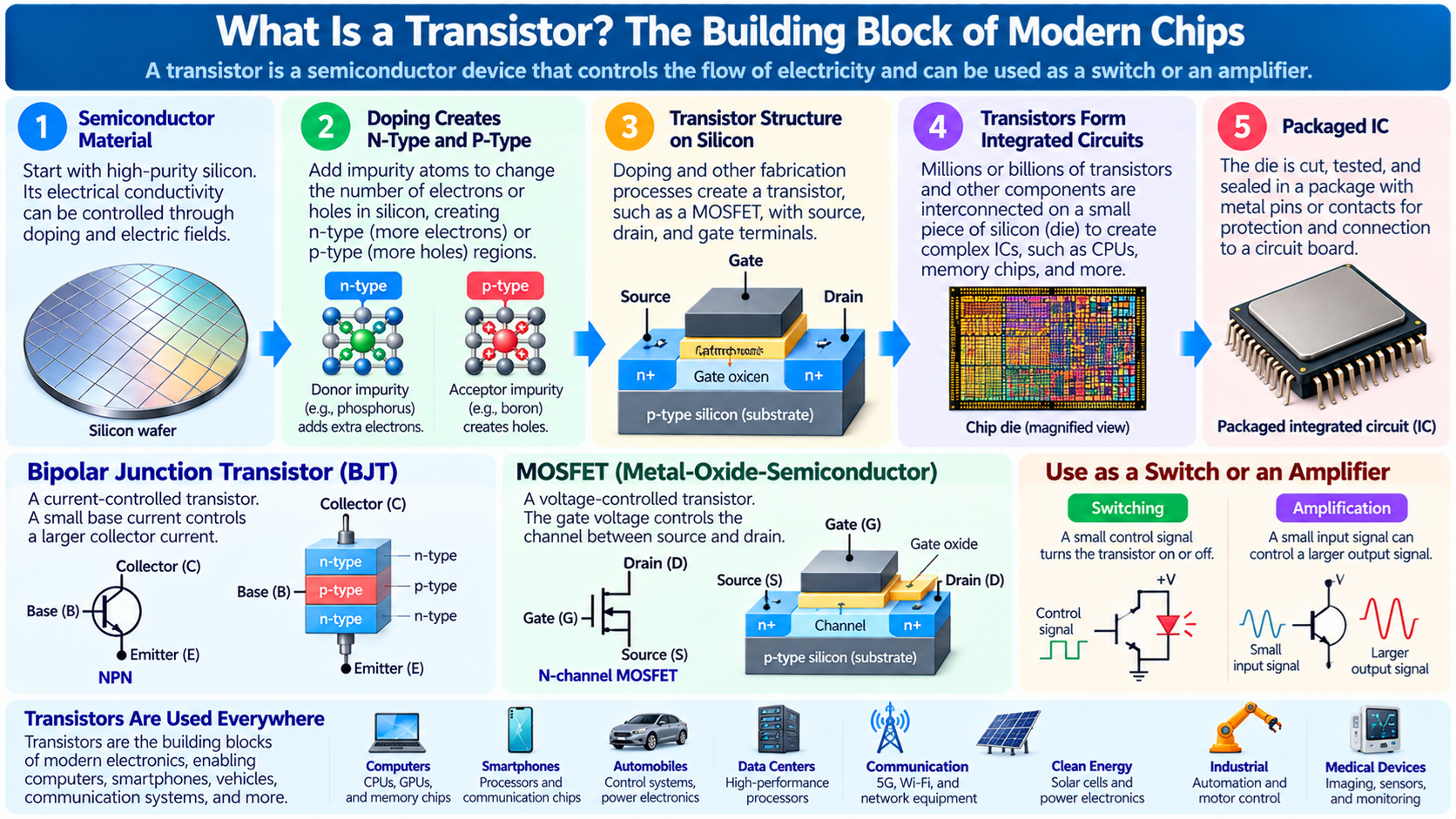
1. What Is a Transistor?
A transistor is a semiconductor device that controls electrical current or voltage.
It is one of the most important inventions in modern electronics and serves as a fundamental building block of computer processors, memory chips, microcontrollers, communication equipment, and many other electronic systems.
Transistors can perform two particularly important functions: switching and amplification.
As an electronic switch, a transistor can control whether current flows through a circuit.
As an amplifier, it can use a relatively small input signal to control a larger electrical signal, using energy supplied by an external power source.
The switching function is especially important in digital electronics.
Modern computers represent and process information using binary values, commonly called 0 and 1.
Transistors can be interconnected to create electronic circuits that manipulate these values.
For example, a simple digital logic gate may contain only a few transistors, while a modern processor can contain billions of them.
These transistors work together to perform arithmetic operations, store information, control data movement, and execute software instructions.
A single transistor cannot execute a software program or perform all the functions of a computer.
Complex computation becomes possible when large numbers of transistors are organized into logic gates, registers, arithmetic units, memory systems, and processors.
Understanding transistors is therefore an essential first step toward understanding how computer chips actually work.
2. Why Was the Transistor Invented?
Before transistors became widely available, many electronic circuits used vacuum tubes to amplify signals and perform switching operations.
Vacuum tubes made early radio systems, electronic amplifiers, and digital computers possible, but they had significant disadvantages.
Vacuum tubes were relatively large, consumed considerable electrical power, generated heat, and often required high operating voltages.
Systems containing thousands of tubes were expensive to build and maintain.
Engineers wanted smaller and more reliable electronic devices that could perform similar functions.
Semiconductor research eventually led to the development of the transistor.
The first successful point-contact transistor was demonstrated at Bell Laboratories in December 1947 by John Bardeen and Walter Brattain, working within a research group led by William Shockley. Shockley subsequently developed the junction transistor concept.
Bardeen, Brattain, and Shockley received the 1956 Nobel Prize in Physics for their research on semiconductors and the discovery of the transistor effect.
The transistor gradually replaced vacuum tubes in many electronic applications.
Its smaller size, lower power requirements, and compatibility with mass production helped transform the electronics industry.
The development of integrated circuits later made it possible to manufacture many transistors together on a single semiconductor die.
This combination of transistor technology and semiconductor integration created the foundation of modern computing.
3. What Is a Transistor Made Of?
Most transistors used in modern digital integrated circuits are manufactured using silicon-based semiconductor technology.
Silicon is a semiconductor material whose electrical properties can be modified through doping, electric fields, and carefully designed device structures.
Doping means introducing controlled quantities of impurity atoms into semiconductor material.
These impurities alter the concentration of mobile electrical charge carriers.
For example, adding suitable donor impurities such as phosphorus to silicon can create n-type semiconductor regions, where electrons are the majority mobile carriers.
Adding suitable acceptor impurities such as boron can create p-type semiconductor regions, where holes are the majority mobile carriers.
A hole is an unoccupied electronic state in the valence band that behaves like a positively charged carrier.
By combining semiconductor regions with different properties, insulating layers, and conductive connections, engineers can create transistors.
A modern transistor is not simply a piece of silicon with three wires attached.
Its operation depends on precisely engineered dimensions, material interfaces, doping profiles, electric fields, and electrical contacts.
Advanced transistors may also use specialized dielectric materials, metal gates, and three-dimensional device structures.
4. How Does a Transistor Actually Work?
The fundamental idea behind a transistor is that one electrical signal controls another electrical quantity.
However, the exact operating mechanism depends on the type of transistor.
In a bipolar junction transistor, or BJT, current and voltage conditions at the base-emitter junction influence the current flowing between the collector and emitter.
In a field-effect transistor, or FET, an electric field produced by a control voltage changes the conductivity of a channel.
For example, consider a simplified enhancement-mode n-channel MOSFET.
When the voltage between its gate and source is sufficiently low, the conductive channel is largely absent, and the drain-to-source current is very small.
When the gate-to-source voltage becomes sufficiently positive, an inversion channel forms, allowing current to flow between the drain and source when a suitable drain-to-source voltage is present.
The transistor can therefore be used to control the electrical connection between two terminals.
Digital circuits exploit this behavior to produce logical states.
Analog circuits may operate transistors in regions where their currents respond continuously to changes in input voltage or current.
The same fundamental semiconductor technology can therefore support both digital switching and analog amplification.
5. What Are the Main Types of Transistors?
There are several transistor families, but two especially important categories are bipolar junction transistors and field-effect transistors.
A bipolar junction transistor, or BJT, uses semiconductor junctions and carrier injection to control current.
BJTs are commonly available as NPN and PNP devices.
A field-effect transistor, or FET, uses an electric field to control conduction through a channel.
The MOSFET, or Metal-Oxide-Semiconductor Field-Effect Transistor, is one of the most widely used FET types.
MOSFETs are particularly important in modern digital integrated circuits because complementary MOS transistor arrangements can implement logic efficiently.
Other transistor structures include junction field-effect transistors, insulated-gate bipolar transistors, and specialized high-frequency devices.
Different transistor technologies are optimized for different operating conditions.
For example, power transistors may be designed to control large currents or withstand high voltages, while tiny transistors inside processors are optimized for dense integration and rapid switching.
The term transistor therefore describes a broad category of electronic devices rather than one universal physical structure.
6. What Is a Bipolar Junction Transistor (BJT)?
A bipolar junction transistor is a semiconductor device commonly built from three differently doped regions.
These regions form either an NPN or PNP structure.
The three terminals are called the emitter, base, and collector.
The emitter participates in supplying carriers, the base controls carrier transport, and the collector collects carriers under normal active operating conditions.
In an NPN transistor operating in its forward-active region, the base-emitter junction is forward biased while the collector-base junction is reverse biased.
Electrons injected from the emitter travel through the thin base region, and many are collected by the collector.
A relatively small base current is associated with a much larger collector current.
In a simplified common-emitter analysis, the collector current is approximately equal to the base current multiplied by the transistor’s current gain, commonly represented by beta.
However, this relationship applies under appropriate operating conditions and is not a universal fixed ratio.
The collector current also depends strongly on the base-emitter voltage, temperature, device characteristics, and the external circuit.
BJTs are widely used in analog amplifiers, switching circuits, signal conditioning, and other electronic applications.
7. What Is the Difference Between NPN and PNP Transistors?
NPN and PNP transistors are two complementary types of bipolar junction transistors.
An NPN transistor consists of an n-type emitter, a p-type base, and an n-type collector.
A PNP transistor consists of a p-type emitter, an n-type base, and a p-type collector.
The two devices have complementary voltage polarities and carrier behavior.
For example, a conventional silicon NPN transistor may operate with its base approximately 0.6 to 0.8 volts above its emitter under common forward-conduction conditions.
A PNP transistor generally requires the opposite base-emitter polarity for comparable forward operation.
These values are approximate and depend on the current, temperature, and device characteristics. They should not be interpreted as exact switching thresholds.
Circuit symbols distinguish NPN and PNP transistors using the direction of an arrow on the emitter terminal.
For an NPN transistor, the emitter arrow points outward.
For a PNP transistor, the emitter arrow points inward.
Both devices can be used as switches or amplifiers.
The choice depends on the required circuit arrangement, supply voltages, signal polarity, and other design considerations.
8. How Does a BJT Work as an Electronic Switch?
A BJT can control a load by changing between operating regions.
For example, an NPN transistor can be used as a low-side switch to control a small indicator LED.
The emitter may be connected to the circuit’s reference ground, while the collector connects to the LED and its current-limiting resistor.
A suitable current applied to the base allows the transistor to conduct between collector and emitter.
With sufficient base drive, the transistor can enter saturation, producing a relatively low collector-emitter voltage.
The LED can then receive current through the external circuit.
When the base drive is removed, the transistor enters cutoff under suitable conditions, and the collector current becomes very small.
The LED turns off.
This arrangement allows a low-power control signal to switch a load.
However, the base must be driven through an appropriate circuit, usually including a resistor to limit base current.
The collector current must also remain within the transistor’s ratings.
For motors, relays, and other inductive loads, additional protective components may be necessary to handle voltage transients.
This is a practical example of transistor switching, but it is different from the CMOS switching structures used inside most modern digital processors.
9. How Does a Transistor Amplify a Signal?
A transistor can also operate as an amplifier.
Amplification means that a variation in an input signal produces a larger variation in an output signal, with the additional signal energy supplied by the circuit’s power source.
For example, a BJT can be configured as a common-emitter amplifier.
A small change in the base-emitter voltage changes the collector current.
When that current flows through an appropriate load, it produces a changing output voltage.
The circuit can therefore amplify a small input voltage signal.
Similarly, a MOSFET can be used in a common-source amplifier, where changes in gate voltage influence drain current.
Amplifier performance depends on the transistor’s operating point, circuit components, supply voltage, load, and frequency characteristics.
Important parameters include gain, bandwidth, input impedance, output impedance, noise, and distortion.
Transistor amplification is essential in audio electronics, radio receivers, sensor interfaces, measurement equipment, and communication systems.
Not all transistor circuits operate as digital switches. Many intentionally operate in continuous regions where small changes in electrical signals matter.
10. What Is a Field-Effect Transistor (FET)?
A field-effect transistor controls conduction through a semiconductor channel using an electric field.
Unlike a conventional BJT, whose operation involves carrier injection through semiconductor junctions, a FET changes the electrical behavior of a channel through a control voltage.
Common FET terminals include the gate, source, and drain.
The gate controls the channel conductivity.
The source and drain provide connections to the channel through which current flows.
One important advantage of insulated-gate FET technologies is that the gate normally requires very little steady-state current.
However, the gate has electrical capacitance, which must be charged and discharged when switching.
This requires transient current and consumes energy.
MOSFETs are the dominant FET technology in modern digital ICs.
They are also widely used in analog circuits, power supplies, motor drivers, and other applications.
11. What Is a MOSFET?
MOSFET stands for Metal-Oxide-Semiconductor Field-Effect Transistor.
A MOSFET uses an insulated gate structure to control the conductivity of a semiconductor channel.
In a conventional planar MOSFET, the gate is separated from the semiconductor channel region by a thin insulating dielectric.
The gate voltage influences the electric field within the semiconductor.
For a typical enhancement-mode n-channel MOSFET, a sufficiently positive gate-to-source voltage allows a conductive inversion channel to form.
Current can then flow between drain and source when the external voltage conditions permit it.
A p-channel MOSFET operates with complementary carrier and voltage behavior.
MOSFETs are suitable for dense integrated circuit manufacturing, and modern digital processors contain enormous numbers of MOS devices.
The name MOSFET is historical. Modern devices may use metal gates and high-k dielectric materials rather than the original simple material structures.
The basic concept remains electric-field control of channel conduction.
12. What Are Gate, Source, and Drain?
A MOSFET typically has three primary external terminals: gate, source, and drain.
It also has a body or substrate connection, which may be externally accessible or internally connected depending on the device.
The gate controls the channel through an electric field.
The source and drain connect to the conductive path controlled by the gate.
For a simplified n-channel enhancement MOSFET, the gate-to-source voltage is commonly written as VGS.
The drain-to-source voltage is written as VDS.
When VGS is below the relevant threshold, the device has relatively low channel conduction.
When VGS increases sufficiently, channel conduction becomes stronger.
The resulting drain current also depends on VDS and the device’s operating region.
The gate threshold voltage does not mean that the transistor suddenly becomes a perfect zero-resistance switch.
A real MOSFET changes behavior continuously, and the transition between weak and strong conduction depends on device physics.
When selecting a MOSFET for a circuit, engineers must examine the datasheet rather than relying only on a simplified gate threshold value.
13. What Is the MOSFET Threshold Voltage?
Threshold voltage is an important parameter in MOSFET operation.
It identifies a gate-voltage condition associated with the formation of a conductive inversion channel according to a particular device definition.
However, threshold voltage is not the same as the gate voltage required to operate a power MOSFET with low resistance.
For example, a power MOSFET datasheet may specify a gate threshold voltage measured at a very small drain current.
A larger gate-to-source voltage may be needed to achieve the low on-resistance specified for switching applications.
The required voltage depends on the specific device.
This distinction is particularly important when controlling MOSFETs from microcontrollers.
A microcontroller output may operate at 3.3 volts, but not every MOSFET is suitable for efficient switching with that gate drive.
The designer should verify the specified on-resistance at the intended gate voltage, along with current, voltage, thermal, and switching requirements.
For integrated digital circuits, threshold voltage is also an important design parameter affecting speed, leakage, and power consumption.
14. What Is the Difference Between BJT and MOSFET?
BJTs and MOSFETs can both function as electronic switches and amplifiers, but they use different operating mechanisms.
A BJT is controlled through the electrical conditions of its semiconductor junctions, with base current playing an important role in conventional circuit operation.
A MOSFET is controlled through the gate voltage and the electric field affecting its channel.
In a BJT, the base-emitter junction normally conducts current when forward biased.
In an insulated-gate MOSFET, the gate ideally has negligible steady-state current, although gate charging and leakage remain relevant.
MOSFETs are widely used in CMOS digital integrated circuits because complementary transistor networks provide efficient logic operation.
BJTs remain important in analog circuitry, certain high-speed applications, and specialized semiconductor technologies.
Power MOSFETs are widely used for efficient electronic switching.
Neither transistor type is universally superior.
The appropriate choice depends on electrical characteristics, operating frequency, power requirements, gain, noise, cost, and the intended application.
15. What Is CMOS Technology?
CMOS stands for Complementary Metal-Oxide-Semiconductor.
It is a circuit technology that uses complementary n-channel and p-channel MOS transistors.
CMOS is particularly important because it enables efficient digital logic circuits.
Consider a basic CMOS inverter, also called a NOT gate.
The circuit contains a p-channel MOSFET connected toward the positive supply and an n-channel MOSFET connected toward ground.
Their gates are connected together to form the input, and their drains form the output.
When the input voltage is low, the p-channel transistor conducts while the n-channel transistor is largely off.
The output is pulled toward the positive supply, producing logic 1.
When the input voltage is high, the n-channel transistor conducts while the p-channel transistor is largely off.
The output is pulled toward ground, producing logic 0.
In an ideal static state, this arrangement avoids a continuous low-resistance conduction path between the positive supply and ground.
Real CMOS circuits still consume leakage power and switching energy.
Nevertheless, CMOS has become the dominant technology for large-scale digital integrated circuits.
16. How Do Transistors Create Logic Gates?
Logic gates are circuits that perform operations on digital signals.
A transistor can control current flow, but several transistors can be connected to create a circuit with a defined logical function.
For example, a CMOS inverter uses two transistors.
A conventional static CMOS two-input NAND gate typically uses four transistors.
A two-input NOR gate can also be implemented using four transistors.
An AND gate can be formed by combining a NAND gate with an inverter.
More complex logic functions may require additional transistors.
An XOR gate produces logic 1 when its two inputs differ.
XOR operations are useful in binary arithmetic, comparison, parity generation, and many other digital circuits.
By combining logic gates, engineers can create adders, multiplexers, decoders, counters, and control systems.
These circuits can then be integrated into processors and other semiconductor chips.
The key principle is that the behavior of larger digital systems can be built from combinations of simpler transistor-based logic functions.
17. How Do Transistors Perform Binary Addition?
Digital arithmetic is implemented using electronic circuits built from logic gates.
Consider adding two one-bit binary values.
The possible input combinations are 0 plus 0, 0 plus 1, 1 plus 0, and 1 plus 1.
In binary arithmetic, 1 plus 1 produces binary 10.
This result contains a sum bit of 0 and a carry bit of 1.
A circuit called a half adder can implement this operation.
The sum output is the XOR of the two input bits.
The carry output is the AND of the two input bits.
A full adder extends this concept by including an incoming carry bit.
Multiple full adders can be combined to create circuits that add larger binary numbers.
For example, a 32-bit arithmetic unit may add two 32-bit operands using a suitable adder structure.
Modern processors use advanced adder architectures to improve timing, power, or area efficiency.
The important idea is that arithmetic operations are implemented physically through transistor switching and circuit connections.
The transistors do not understand mathematics. Their electrical behavior implements the logical relationships required by binary arithmetic.
18. How Do Transistors Store Binary Information?
Digital circuits must often remember information rather than simply calculate an output from current inputs.
This requires storage elements.
One example is a latch, which can preserve a logical state under appropriate control conditions.
Another example is a flip-flop, which commonly captures data in response to a clock edge.
Flip-flops are used to construct registers that store binary values.
For example, a 32-bit register contains enough storage elements to preserve 32 bits of information.
Transistor circuits can also form memory cells.
A common SRAM cell uses six transistors to store one bit while power is supplied.
The storage element typically includes cross-coupled inverters and access transistors.
DRAM uses a different approach, generally storing data as electrical charge in capacitive cells accessed through transistors.
Flash memory uses nonvolatile semiconductor storage structures.
These technologies demonstrate that transistors are essential not only for calculation but also for retaining digital information.
19. How Are Transistors Used in CPUs?
A CPU is a complex integrated circuit designed to execute machine instructions.
Modern CPU cores contain logic circuits, registers, arithmetic units, instruction processing structures, caches, and control systems.
These components are constructed from large numbers of transistors.
For example, when a CPU executes an ADD instruction, it may read operands from registers, process them through arithmetic circuitry, and store the result.
A branch instruction uses control and comparison logic to determine the next instruction path.
A load instruction involves address calculation and communication with the memory hierarchy.
Modern CPUs may execute several instructions concurrently using pipelining and other architectural techniques.
Caches contain large arrays of transistor-based memory cells.
Clock distribution and power management also require extensive circuitry.
The operation of an entire processor therefore depends on the coordinated behavior of enormous numbers of transistors.
However, transistor count alone does not determine processor performance.
Architecture, clock speed, memory behavior, power limits, and software workloads also matter.
20. How Are Transistors Used in GPUs?
A GPU, or Graphics Processing Unit, is designed to provide high computational throughput for graphics and suitable parallel workloads.
Like a CPU, a GPU is constructed from semiconductor transistors.
However, its architecture allocates resources differently.
A GPU typically contains many arithmetic execution resources designed to perform similar operations across large collections of data.
For example, graphics rendering involves processing vertices, pixels, textures, and other data.
Artificial intelligence workloads often involve matrix multiplication and other parallel numerical operations.
Transistors within a GPU form arithmetic units, register files, caches, control circuits, and specialized processing structures.
Modern GPUs may also contain dedicated hardware for matrix operations, ray tracing, video processing, and other functions.
The transistor technology may be similar to that used in CPUs, but the architecture is designed for different performance objectives.
This illustrates an important distinction: semiconductor transistors provide the building blocks, while the organization of those blocks determines the capabilities of the processor.
21. How Are Transistors Used in Memory Chips?
Memory chips use semiconductor devices to store information.
Different memory technologies employ different cell structures.
SRAM uses transistor-based circuits that maintain stored states while power is supplied.
DRAM uses capacitive storage cells and access transistors, requiring periodic refresh because stored charge leaks away.
NAND flash memory uses nonvolatile storage cells whose programmed states remain available without continuous external power.
Modern storage technologies can represent information through charge or other device states, depending on the memory architecture.
Memory density depends on the cell structure, manufacturing technology, and the organization of the memory array.
For example, modern NAND flash commonly uses three-dimensional arrangements of memory cells to increase capacity.
Transistors also appear in memory decoders, sense amplifiers, control logic, and interface circuits.
Therefore, memory chips rely on semiconductor devices for both storage and the supporting operations required to read and write information.
22. What Are Power Transistors?
Power transistors are semiconductor devices designed to control significant amounts of electrical power.
They are used in power supplies, motor controllers, inverters, battery management systems, and industrial equipment.
Common examples include power MOSFETs and insulated-gate bipolar transistors, or IGBTs.
Unlike the extremely small logic transistors used inside dense processor cores, power transistors are optimized for handling higher currents, voltages, or thermal loads.
For example, a switching power supply uses transistors to rapidly control the transfer of electrical energy.
By switching efficiently and using suitable energy-storage components, the circuit can convert electrical power from one voltage level to another.
Power transistors also drive motors and other electrical loads.
Their performance depends on conduction losses, switching losses, voltage ratings, current ratings, thermal behavior, and control circuitry.
A transistor that is suitable for high-speed digital logic is not automatically appropriate for switching a large motor.
Device structure and application requirements determine the best transistor technology.
23. What Are Silicon Carbide and Gallium Nitride Transistors?
Although silicon dominates mainstream digital integrated circuits, other semiconductor materials are important in certain applications.
Silicon carbide, or SiC, is a wide-bandgap semiconductor used in high-voltage and high-power electronic devices.
Its material properties can provide advantages in power conversion systems, including certain electric vehicle inverters and industrial power applications.
Gallium nitride, or GaN, is another wide-bandgap semiconductor material.
GaN-based transistors are used in selected high-frequency, radio-frequency, and power conversion applications.
For example, some compact power adapters use GaN power devices to support efficient high-frequency switching.
However, SiC and GaN are not universal replacements for silicon.
Their advantages depend on operating voltage, frequency, thermal requirements, cost, packaging, and the rest of the circuit design.
Silicon remains highly competitive in many power and general-purpose electronic applications.
Different semiconductor materials provide engineers with different performance and design options.
24. Why Are Modern Transistors So Small?
The semiconductor industry has spent decades improving manufacturing technology to integrate more transistors into limited chip area.
Smaller devices can allow higher transistor density and may enable improvements in speed, energy efficiency, and functionality.
However, reducing transistor dimensions is not a simple geometric process.
As structures become smaller, electric fields, leakage currents, parasitic capacitances, and manufacturing variations become increasingly important.
Interconnect delay can also limit the benefit of faster transistor switching.
Modern transistor designs use sophisticated structures and materials to manage these effects.
Advanced manufacturing requires extremely precise lithography, deposition, etching, and measurement processes.
It is also important to understand that semiconductor process labels such as 7 nm, 5 nm, or 3 nm do not necessarily represent one physical transistor dimension.
Modern process node names are primarily technology generation labels.
A newer process may offer useful improvements, but actual chip performance depends on architecture and implementation as well as transistor technology.
25. What Is a FinFET?
FinFET stands for Fin Field-Effect Transistor.
It is a transistor structure developed to improve electrostatic control as semiconductor dimensions became smaller.
Traditional planar MOSFETs use a relatively flat channel structure.
A FinFET uses a raised fin-shaped semiconductor channel.
The gate controls the channel from multiple sides.
This geometry improves control over the channel compared with a comparable traditional planar transistor.
Better electrostatic control helps manage short-channel effects and unwanted leakage.
FinFETs have been widely used in advanced digital semiconductor processes.
However, FinFET manufacturing requires additional design and fabrication complexity.
The transistor’s fin geometry, gate structure, contacts, and interconnections must be carefully engineered.
FinFET technology illustrates how improving semiconductor performance involves changing device architecture rather than simply reducing dimensions.
26. What Is a GAAFET?
GAAFET stands for Gate-All-Around Field-Effect Transistor.
It is an advanced transistor structure in which the gate surrounds the conductive channel more completely.
GAAFET implementations may use nanosheets or nanowires.
Compared with a similar FinFET, a suitable GAAFET structure can provide improved electrostatic control over the channel.
This can help manage leakage and support further transistor scaling.
However, the manufacturing process is complex.
The channel geometry, gate materials, insulating layers, and contact structures require precise fabrication.
Different semiconductor manufacturers may use different implementations and naming conventions.
GAAFETs represent one of the major developments in advanced transistor design, but not every semiconductor product needs this technology.
Many useful chips continue to be manufactured using older planar or FinFET processes.
27. What Is Transistor Switching Speed?
Transistor switching speed describes how quickly a device can change its electrical state under particular conditions.
In digital circuits, switching speed contributes to the time required for signals to propagate through logic gates.
However, a transistor does not switch instantaneously.
Electrical capacitances must be charged or discharged, and the conducting channel responds according to device characteristics and applied voltages.
The external circuit also matters.
For example, a transistor driving a large capacitive load may switch the output more slowly than the same transistor driving a small load.
In integrated circuits, propagation delay depends on transistor strength, interconnect capacitance, supply voltage, temperature, and other factors.
A processor’s maximum operating frequency is determined by timing across complete circuit paths, not by the speed of one isolated transistor.
Engineers therefore analyze both transistor behavior and system-level timing when designing high-performance chips.
28. Why Do Transistors Consume Power?
Transistors consume power through several mechanisms.
In CMOS digital circuits, one important component is dynamic power consumption caused by switching.
When an output changes logical state, electrical capacitances are charged or discharged.
The energy associated with these operations contributes to dynamic power.
A common simplified relationship is:
P ≈ αCV²f
Here, P represents dynamic power, α represents switching activity, C represents effective switched capacitance, V represents supply voltage, and f represents switching frequency.
This relationship shows why higher voltage and increased switching activity can increase power consumption.
Transistors also consume leakage power.
Even when a transistor is considered off, small currents may still flow.
In analog circuits, transistors may intentionally conduct bias currents continuously.
Power transistors also dissipate energy through conduction and switching losses.
The total power consumption of a chip therefore depends on its circuitry, operating conditions, workload, and manufacturing technology.
29. Why Do Transistors Generate Heat?
Electrical energy dissipated within semiconductor devices is converted into heat.
In digital chips, transistor switching and leakage contribute to thermal power.
In power electronics, conduction resistance, voltage drops, and switching transitions also generate heat.
As transistor density and computational activity increase, removing heat becomes a significant engineering challenge.
A processor may contain billions of transistors operating within a relatively small area.
If too much heat accumulates, transistor characteristics can change and device reliability may be affected.
Modern processors use thermal sensors and power management circuits to monitor operating conditions.
When temperature or power limits are approached, the processor may reduce frequency, voltage, or activity.
This helps keep the device within its supported operating range.
The external system may use a heat spreader, heatsink, fan, or liquid cooling system.
Efficient thermal management is therefore essential for high-performance semiconductor devices.
30. How Are Transistors Manufactured?
Modern transistors are manufactured using highly specialized semiconductor fabrication processes.
The process begins with semiconductor wafers, commonly made from highly purified single-crystal silicon.
Many transistor structures and complete integrated circuits are fabricated across the wafer.
Manufacturing includes operations such as lithography, deposition, etching, ion implantation, annealing, and polishing.
Lithography defines patterns used in later processing steps.
Deposition creates thin layers of materials.
Etching removes selected regions.
Ion implantation introduces dopants into semiconductor regions.
Annealing can activate dopants and help repair certain crystal damage caused by processing.
Additional steps create gate structures, source and drain regions, electrical contacts, and interconnections.
Modern transistors require precise control over device geometry and material properties.
After the circuit layers are manufactured, the wafer is tested and separated into individual dies.
These dies are then packaged for use in electronic systems.
The fabrication process is one of the reasons modern transistor technology requires advanced industrial equipment and extensive engineering expertise.
31. How Are Billions of Transistors Connected Inside a Chip?
Modern integrated circuits contain multiple layers of electrical interconnections.
Transistors are formed in or near the semiconductor substrate.
Conductive structures above the devices connect them into logic gates, memory cells, and larger circuit blocks.
These connections use carefully designed metal layers separated by insulating materials.
Vertical connections called vias connect different routing layers.
Short local interconnections join nearby transistors.
Larger connections link functional blocks, distribute clock signals, and supply electrical power.
The interconnection network is extremely important because electrical signals require time to travel through the circuit.
Long wires introduce resistance and capacitance.
These effects can increase propagation delay and power consumption.
Modern electronic design automation tools help engineers place circuit elements and route their connections.
Therefore, building a powerful chip requires more than manufacturing fast transistors.
Engineers must also organize and connect the transistors efficiently.
32. How Are Transistors Designed Using Verilog?
Verilog is a hardware description language used to describe digital circuits.
Engineers often use Verilog or SystemVerilog to describe logic at the Register Transfer Level, commonly called RTL.
For example, an RTL description may specify how a counter updates on each clock edge or how an arithmetic unit calculates a result.
The RTL code does not usually describe every transistor individually.
Instead, it describes logical behavior and relationships between registers and combinational circuits.
Electronic design automation tools can synthesize the RTL into a network of logic cells.
For an ASIC, these logic cells are mapped to a semiconductor technology library.
The resulting cells contain transistor-level circuit implementations.
Physical design tools then place the cells and create interconnections.
For an FPGA, synthesis and implementation tools map the digital design into available configurable logic and routing resources.
The FPGA already contains manufactured transistors, so programming the FPGA changes its configuration rather than physically manufacturing new transistors.
This distinction is important when learning the relationship between software-like hardware descriptions and actual electronic circuits.
33. What Is the Difference Between a Transistor and a Logic Gate?
A transistor is a semiconductor device that controls electrical behavior.
A logic gate is a circuit that implements a defined logical function.
A logic gate may contain several transistors connected in a particular arrangement.
For example, a conventional CMOS inverter contains two transistors.
A two-input static CMOS NAND gate typically contains four transistors.
More complicated gates may contain additional devices.
A transistor alone does not automatically perform an AND or XOR operation.
The logical behavior depends on the arrangement of the transistor network and how its inputs and outputs are connected.
Logic gates can then be combined into larger circuits.
Adders use logic gates to perform arithmetic.
Multiplexers select signals.
Registers preserve logical states.
Processors combine these functions into instruction execution hardware.
The transistor is therefore a physical semiconductor building block, while the logic gate is a functional circuit constructed from such building blocks.
34. What Is the Difference Between a Transistor and an Integrated Circuit?
A transistor is an individual semiconductor device.
An integrated circuit, or IC, is a manufactured electronic circuit containing multiple components and interconnections.
For example, a discrete transistor may be packaged as a small component with three terminals.
An integrated circuit may contain many transistors and other components on one semiconductor die.
A simple logic IC may contain only a relatively small number of transistors.
A modern processor IC may contain billions.
The integrated circuit also includes the electrical connections needed for the components to work together.
In other words, transistors provide individual electronic functions, while integrated circuits combine them into useful systems.
Not every IC consists only of transistors.
Analog and mixed-signal ICs may also contain integrated resistors, capacitors, diodes, and other structures.
The relationship between transistor and IC is similar to the relationship between a building component and a complete engineered structure.
35. Can a Transistor Be Used Without a Computer?
Transistors are used in many applications that do not involve conventional computers.
For example, a transistor can control an LED, amplify an audio signal, or switch a relay.
Power transistors control motors, electrical converters, and power supplies.
Radio-frequency transistors amplify or process signals in communication equipment.
Analog transistors are used in sensors, measurement instruments, and audio electronics.
A simple transistor circuit can operate entirely without software.
For example, a transistor-based amplifier responds continuously to its electrical input according to its circuit design.
A transistor oscillator can generate periodic signals.
A switching circuit can respond to a sensor or control voltage.
These examples demonstrate that transistors are fundamental electronic devices, not components used exclusively inside CPUs.
36. Are All Transistors Made from Silicon?
Silicon is the most common semiconductor material used for general-purpose digital transistors, but it is not the only material.
Germanium was important in early transistor development and remains useful in selected semiconductor technologies.
Silicon-germanium technologies are used in certain high-frequency and mixed-signal applications.
Gallium arsenide is used in some high-frequency and optoelectronic devices.
Gallium nitride is important in selected radio-frequency and power applications.
Silicon carbide is widely used for certain high-voltage power devices.
Different semiconductor materials provide different band gaps, carrier transport properties, thermal characteristics, and manufacturing trade-offs.
The choice of material depends on the application.
For example, a processor optimized for dense digital logic has different requirements from a transistor used in a high-voltage electric vehicle inverter.
No single semiconductor material is optimal for every transistor application.
37. Are More Transistors Always Better?
A larger transistor count does not automatically mean a chip will perform better in every application.
Transistors can be used for many purposes, including arithmetic circuitry, control logic, memory, caches, and specialized accelerators.
A processor with a larger cache may contain more transistors without necessarily having proportionally more arithmetic capability.
A GPU may contain many transistors dedicated to parallel computation and graphics functions.
A microcontroller may use relatively few transistors but provide excellent efficiency for a small embedded application.
Performance also depends on clock frequency, architecture, software, memory bandwidth, interconnects, and thermal limits.
For example, a poorly optimized program may fail to use additional processing resources effectively.
A chip with fewer transistors but a more suitable architecture may outperform a larger chip on a particular workload.
Transistor count indicates the scale of semiconductor integration, not a universal measure of usefulness or performance.
38. What Is Moore’s Law?
Moore’s Law is an observation associated with Gordon Moore, who described a historical trend in the increasing complexity of integrated circuits.
In 1965, Moore observed that the number of components economically integrated onto semiconductor chips had been increasing rapidly.
The observation was later commonly expressed as the expectation that transistor counts on integrated circuits would approximately double over a period of about two years.
Moore’s Law is not a physical law.
It describes a technological and economic trend rather than a guarantee that transistor density will always increase at a fixed rate.
Over time, semiconductor development has faced growing challenges involving manufacturing cost, device physics, power density, and interconnect performance.
The industry has responded through changes in transistor structures, process technology, architecture, and packaging.
Advanced chiplet designs and three-dimensional integration provide additional ways to increase system complexity.
Moore’s Law remains historically important because it helps explain the remarkable growth of semiconductor capability over many decades.
39. What Happens When Transistors Become Extremely Small?
As transistor dimensions become smaller, several physical effects become more important.
One challenge involves leakage current.
A transistor that is nominally off may still conduct a small current.
Another challenge involves electrostatic control over the channel.
As channel dimensions shrink, the drain and other device regions can influence the channel in ways that complicate gate control.
Quantum mechanical effects, including tunneling through very thin barriers, may also become relevant.
Manufacturing variation becomes more significant because small dimensional differences can affect device characteristics.
Interconnection resistance and capacitance can limit performance even when transistor switching improves.
These challenges have encouraged the development of new transistor structures such as FinFETs and GAAFETs.
Semiconductor engineers also use improved materials, sophisticated design methods, and advanced packaging techniques.
Transistor scaling is therefore an engineering process involving many competing electrical and manufacturing constraints.
40. What Are the Most Important Transistor Specifications?
When selecting a transistor for a practical circuit, engineers must examine the device’s electrical specifications.
For a MOSFET, important parameters may include maximum drain-source voltage, allowable drain current, gate-source voltage limits, on-resistance, gate charge, and thermal resistance.
For a BJT, important parameters may include maximum collector-emitter voltage, collector current, power dissipation, current gain characteristics, and switching behavior.
The transistor’s operating temperature range is also important.
Datasheets typically distinguish between absolute maximum ratings and recommended operating conditions.
Absolute maximum ratings describe limits that should not be exceeded.
They do not represent preferred everyday operating conditions.
For power applications, thermal design is essential because the transistor may dissipate considerable energy.
For high-frequency applications, device capacitances, gain, and frequency response become important.
For digital logic, switching delay, leakage current, and power consumption are major concerns.
The correct transistor depends on the circuit’s actual requirements, not simply on whether the device is described as fast or powerful.
41. How Can Beginners Experiment with Transistors?
A simple transistor switching circuit is a useful beginner project.
For example, a low-voltage NPN transistor can be used to control an LED.
The circuit requires a suitable transistor, a current-limiting resistor for the LED, a base resistor, and an appropriate low-voltage DC power supply.
A small control voltage applied through the base resistor can turn the transistor on under suitable conditions.
Removing the base drive turns the transistor off.
This demonstrates how an electrical control signal can influence current through a separate load path.
A MOSFET can be used for a similar experiment, although the gate drive requirements differ.
For beginners, it is important to stay within the device’s voltage, current, and power ratings.
Do not connect experimental transistor circuits directly to household AC mains.
Circuit simulators are another useful learning tool.
They allow students to examine transistor voltage, current, and switching behavior without immediately building physical hardware.
Once basic switching is understood, students can explore logic gates, amplifiers, oscillators, and digital storage elements.
These experiments connect semiconductor theory with practical electronics.
42. How Should Beginners Learn Transistor Technology?
A practical learning path begins with basic electrical concepts.
First, understand voltage, current, resistance, and electrical power.
Next, study semiconductor materials and the meaning of electrons, holes, and doping.
Learn how p-type and n-type regions are formed.
Then study PN junctions and semiconductor diodes.
After that, learn the operating principles of BJTs and MOSFETs.
Understand the difference between using a transistor as a switch and using it as an amplifier.
Next, explore CMOS logic.
Begin with a NOT gate and then study NAND, NOR, AND, OR, and XOR functions.
Once logic gates are familiar, learn how they form adders, multiplexers, flip-flops, counters, and registers.
These concepts provide the foundation for understanding CPUs, GPUs, memory chips, FPGAs, and ASICs.
For more advanced study, explore transistor device physics, circuit simulation, semiconductor manufacturing, and integrated circuit physical design.
The most important objective is to connect the physical operation of a transistor with the logical behavior of larger electronic circuits.
43. Common Misunderstandings About Transistors
One common misunderstanding is that every transistor is simply an on/off switch.
Transistors can operate as switches, but they can also amplify signals and perform other analog functions.
Another misconception is that a transistor directly represents one binary bit.
A transistor can contribute to a circuit that stores or processes binary information, but a complete storage element or logic function often requires multiple transistors.
Some beginners assume that the MOSFET gate threshold voltage is the exact voltage required for full conduction.
In reality, threshold voltage is defined under particular measurement conditions and does not necessarily indicate a suitable gate drive voltage for low-resistance switching.
Another misunderstanding is that a BJT always provides a fixed current gain.
Actual BJT current gain varies with operating current, temperature, device characteristics, and operating region.
It is also incorrect to assume that smaller transistors always consume less total power.
Power depends on switching activity, voltage, frequency, leakage, and circuit architecture.
Finally, transistor count alone does not determine the performance of a processor.
The arrangement and operation of the transistors are just as important as their number.
44. Why Is the Transistor the Building Block of Modern Chips?
The transistor is considered the building block of modern chips because it provides the controllable electrical behavior required for digital logic, memory, amplification, and many other electronic functions.
A transistor can influence electrical current.
Several transistors can form a logic gate.
Logic gates can be combined into arithmetic circuits and control systems.
Transistor-based storage elements can preserve binary states.
These circuits can be organized into processor cores, memory arrays, communication interfaces, and specialized accelerators.
Semiconductor manufacturing allows enormous quantities of these devices to be fabricated and interconnected on a small die.
For example, modern CPUs and GPUs contain billions of transistors arranged into complex functional structures.
Integrated circuits also include analog and mixed-signal devices that use transistors for amplification, sensing, regulation, and signal processing.
The transistor’s importance comes from both its electrical functionality and its ability to be manufactured in large numbers with highly controlled characteristics.
Without transistors, the compact, efficient, and programmable electronic systems used today would not exist in their current form.
45. Conclusion: How Does a Transistor Actually Work?
A transistor is a semiconductor device that controls electrical current or voltage.
Two of its most important applications are switching and amplification.
Bipolar junction transistors use semiconductor junction behavior and carrier injection, while field-effect transistors control channel conduction through electric fields.
MOSFETs are especially important in modern digital integrated circuits.
By combining complementary n-channel and p-channel MOSFETs, engineers create CMOS logic circuits that process binary signals.
Logic gates form arithmetic circuits, registers, control systems, and memory structures.
These larger components form CPUs, GPUs, microcontrollers, memory chips, and other complex integrated circuits.
Modern semiconductor manufacturing allows billions of transistors to be fabricated within compact devices.
Advanced technologies such as FinFETs and GAAFETs continue improving transistor structures as semiconductor scaling becomes more challenging.
Transistors are also essential in analog amplifiers, radio-frequency circuits, power supplies, motor controllers, electric vehicles, and industrial equipment.
The most important principle is simple: a transistor controls electrical behavior, and by connecting enormous numbers of transistors into carefully designed circuits, engineers create the logic, memory, and processing systems that make modern computer chips work.
Understanding the transistor is therefore one of the most important foundations for studying digital electronics, computer architecture, semiconductor manufacturing, FPGA development, and ASIC design.