Detailed Beginner Guide to RV32I: The Base Integer Instruction Set of RISC-V
RV32I is the mandatory base 32-bit integer instruction set in the RISC-V architecture. It contains approximately 47 instructions and forms the foundation for every RISC-V processor.
Its design is simple, regular, and highly suitable for FPGA implementation.
Want to build your own RISC-V CPU from scratch on an FPGA?
Start here with RV32I — the foundational 32-bit integer instruction set of RISC-V.
Simple. Clean. Perfect for learning.
Here’s everything you need to know in one thread:
1/6 pic.twitter.com/lrCYA9Jmtp
— IC and CS Tutorial (@riscvprogram) April 1, 2026
1. The Register File (32 Registers)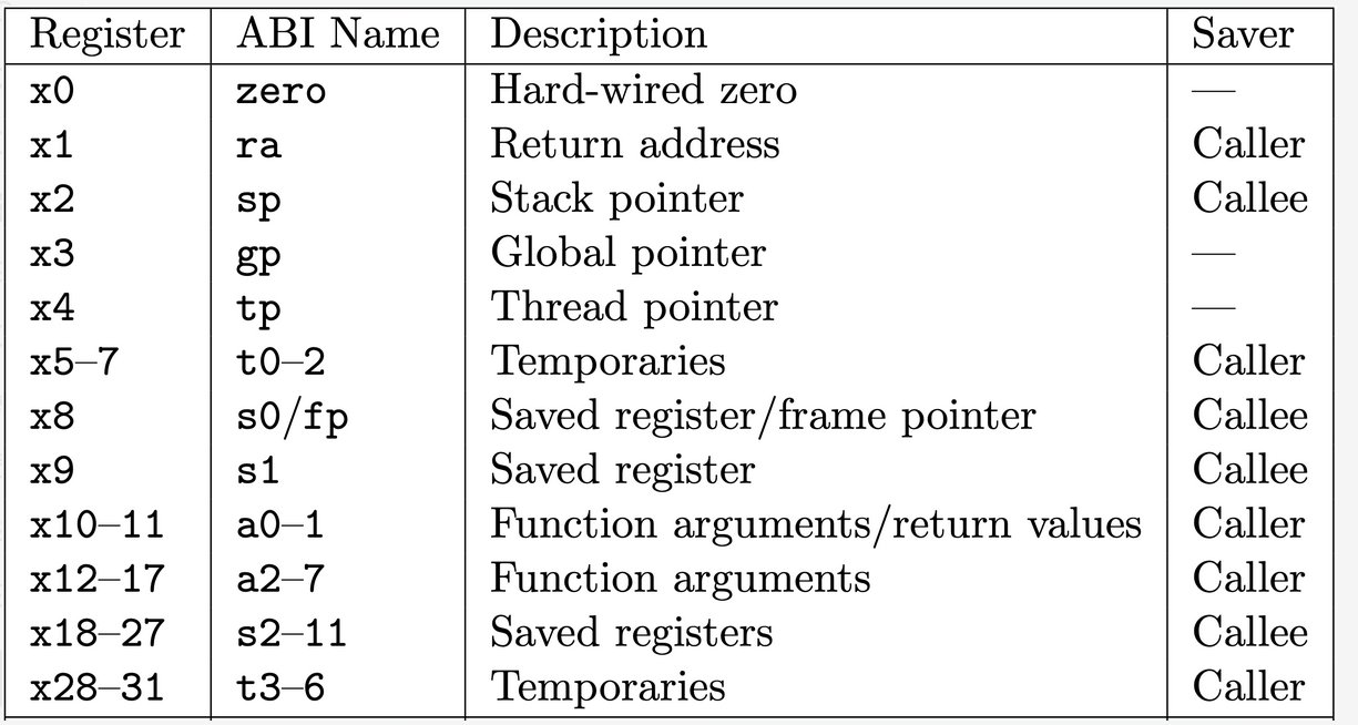
RV32I provides 32 general-purpose 32-bit registers labeled x0 to x31.
x0(also calledzero) is hardwired to 0 and cannot be written.- The remaining 31 registers are fully general-purpose.
Compilers and assemblers use standard ABI names (Application Binary Interface):
x0=zero— always zerox1=ra— return addressx2=sp— stack pointerx3=gp— global pointerx4=tp— thread pointerx5–x7=t0–t2— temporary registersx8–x9=s0–s1— saved registersx10–x17=a0–a7— function arguments and return valuesx18–x27=s2–s11— saved registersx28–x31=t3–t6— temporary registers
Tip: Always prefer ABI names when writing assembly (e.g., addi a0, zero, 42).
2. RV32I Instruction Formats
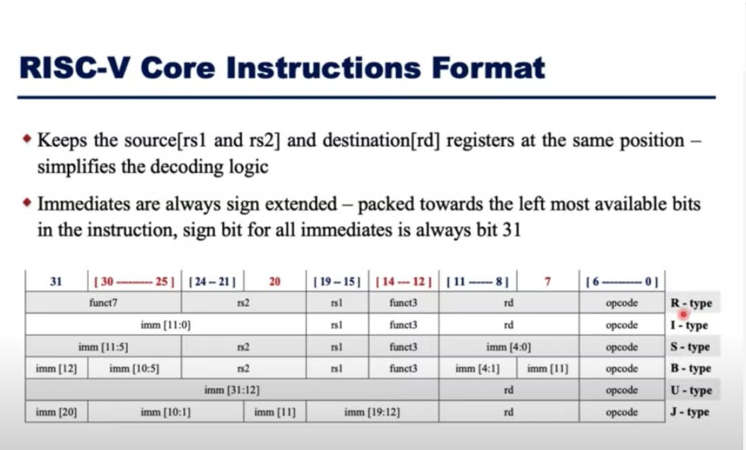
Every RV32I instruction is exactly 32 bits long. There are six main formats:
funct7 | rs2 | rs1 | funct3 | rd | opcodeimm[11:0] | rs1 | funct3 | rd | opcodeimm[11:5] | rs2 | rs1 | funct3 | imm[4:0] | opcodeimm[12|10:5] | rs2 | rs1 | funct3 | imm[4:1|11] | opcodeimm[31:12] | rd | opcodeimm[20|10:1|11|19:12] | rd | opcode3. RV32I Instructions Overview
Arithmetic & Logical (Register-Register)
add rd, rs1, rs2— rd = rs1 + rs2sub rd, rs1, rs2— rd = rs1 – rs2and, or, xorsll, srl, sra— logical/arithmetic shifts
Arithmetic & Logical with Immediate
addi rd, rs1, imm— most frequently used instructionandi, ori, xorislli, srli, srai
Compare and Set
slt / slti— set less than (signed)sltu / sltiu— set less than unsigned
Load and Store
Loads (I-type):
lb/lbu(byte, signed/unsigned)lh/lhu(halfword)lw(word)
Stores (S-type):
sb, sh, sw
beq, bneblt, bge(signed)bltu, bgeu(unsigned)
Jumps
jal rd, imm— jump and linkjalr rd, rs1, imm— jump and link register
Upper Immediate
lui rd, imm— load upper immediateauipc rd, imm— add upper immediate to PC
System Instructions
ecall, ebreak -(environment call / break)
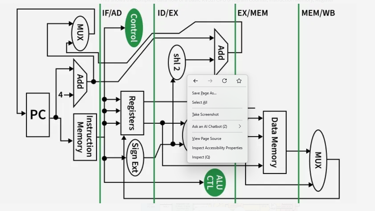
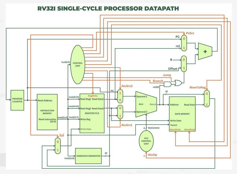
4. How to Build These in Your FPGA CPU (Single-Cycle View)
In a basic single-cycle RISC-V CPU on FPGA, you need these major components:
In a basic single-cycle RISC-V CPU you implement:
- Instruction Fetch → PC → Instruction Memory
- Decode → extract rs1, rs2, rd, opcode, funct3, funct7, immediate
- Register File → read rs1/rs2
- Immediate Generator → create correct 32-bit immediate based on format
- ALU → perform add/sub/logic/shift/compare
- Data Memory → for loads/stores
- Writeback → write result back to rd
- Next PC logic → for branches/jumps
Here are visual examples of the single-cycle datapath:
5. Implementation Tips for FPGA
- Start by implementing the ALU (add/sub/logic/shifts/slt).
- Build the Immediate Generator (different wiring for each instruction format).
- Create the Register File.
- Implement the Control Unit (combinational logic based on opcode + funct3 + funct7).
- Test each instruction thoroughly in simulation before synthesizing.
Bruno Levy’s learn-fpga tutorial adds instructions gradually — highly recommended for beginners.
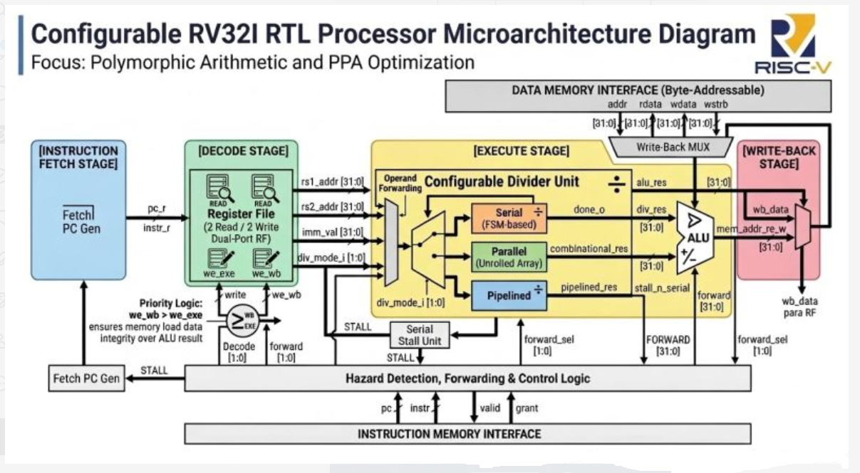
6. Configurable RV32I RTL Processor Microarchitecture Diagram
Ready to Code?
Next logical steps:
- Implement and test
addiandadd. - Add load/store instructions.
- Implement branches and jumps.
This is Great, Thanks