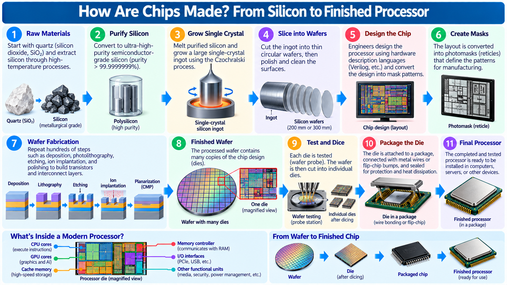
1. How Are Computer Chips Made?
Computer chips are manufactured through an extremely complex process that transforms highly purified semiconductor materials into electronic circuits containing millions or billions of transistors.
These transistors are connected to form processors, memory devices, communication circuits, and many other semiconductor products.
A modern processor begins as an electronic design created by engineers.
That design is converted into physical patterns, and those patterns are manufactured on a thin silicon wafer using specialized semiconductor fabrication equipment.
The wafer undergoes many processing steps, including material deposition, photolithography, etching, doping, transistor formation, and metal interconnection.
Each processing operation helps create part of the electronic structure.
Many operations are repeated to construct the numerous device and wiring layers required by a modern integrated circuit.
Once fabrication is complete, the wafer is electrically tested and separated into individual semiconductor dies.
The usable dies are then packaged, connected to external terminals, and subjected to additional testing.
The finished processor can finally be installed in a computer, server, smartphone, or other electronic system.
Although a processor may appear to be a small piece of metal and plastic, the actual electronic circuitry inside it represents the result of highly advanced materials science, semiconductor physics, computer engineering, and industrial manufacturing.
This guide explains the complete journey from silicon material to finished processor, including how wafers are made, how transistors are formed, how circuits are connected, and why semiconductor manufacturing is so technologically demanding.
2. Why Are Most Computer Chips Made from Silicon?
Silicon is the most widely used semiconductor material for modern digital integrated circuits.
Its electrical properties make it suitable for manufacturing transistors, the fundamental switching devices used in computer processors and memory chips.
A semiconductor is a material whose electrical conductivity can be controlled through methods such as doping and electric-field manipulation.
Doping introduces carefully selected impurities that change the concentration of mobile charge carriers within the semiconductor.
This makes it possible to create transistor structures that control the flow of electrical current.
Silicon also forms useful insulating materials, particularly silicon dioxide, which has played an important role in the development of integrated circuit manufacturing.
Another advantage is the extensive industrial knowledge developed around silicon processing.
Manufacturers have spent decades improving silicon crystal growth, wafer preparation, transistor fabrication, and integrated circuit production.
These improvements support high-volume manufacturing with precise control over device characteristics.
However, silicon is not the only semiconductor material.
Silicon carbide, gallium nitride, gallium arsenide, and other materials are used in specialized power, radio-frequency, and optoelectronic applications.
For mainstream CPUs, GPUs, and many digital integrated circuits, silicon remains the dominant foundation.
3. Step 1: Extracting Silicon from Raw Materials
The journey of a silicon chip begins with silicon-containing raw materials, commonly including high-purity quartz.
Silicon is abundant in the Earth’s crust, but it is usually found chemically combined with oxygen or other elements rather than as pure silicon.
Quartz contains silicon dioxide, represented by the chemical formula SiO₂.
To obtain silicon, manufacturers use high-temperature industrial processes that separate silicon from oxygen.
One important production method involves heating quartz with carbon in an electric furnace.
This produces metallurgical-grade silicon.
Metallurgical-grade silicon is useful for various industrial purposes, but it is not pure enough for manufacturing advanced electronic devices.
Semiconductor fabrication requires exceptionally low concentrations of unwanted impurities.
Even very small amounts of contamination can alter the electrical behavior of semiconductor devices or reduce manufacturing yield.
Therefore, the silicon must undergo additional purification before it can be used to manufacture electronic-grade wafers.
This is the first important distinction between ordinary industrial silicon and semiconductor manufacturing materials.
The raw material is relatively common, but converting it into material suitable for advanced integrated circuits requires sophisticated processing.
4. Step 2: Purifying Silicon to Electronic Grade
Semiconductor manufacturing requires silicon with extremely high purity.
Unwanted metallic impurities and other contaminants can introduce electrical defects, influence charge carrier behavior, or interfere with device operation.
To produce electronic-grade silicon, manufacturers use specialized chemical purification processes.
One established industrial route converts metallurgical-grade silicon into a silicon-containing chemical compound that can be purified and then converted back into high-purity silicon.
For example, the Siemens process uses chemical vapor deposition to produce highly purified polycrystalline silicon from suitable precursor gases.
Electronic-grade silicon can reach purity levels exceeding 99.9999999 percent, depending on the material specification and production process.
However, purity is not described adequately by one percentage alone.
Different impurities have different effects, and semiconductor manufacturers control particular contaminant concentrations according to strict material requirements.
The purified silicon provides the starting material for growing the large single crystals used in wafer manufacturing.
The goal is to produce silicon with highly controlled chemical composition and crystal quality.
Without this level of purification, manufacturing billions of reliable microscopic devices on one wafer would be impractical.
5. Step 3: Growing a Single-Crystal Silicon Ingot
After purification, the silicon must be converted into a crystal structure suitable for semiconductor fabrication.
Modern integrated circuits generally use single-crystal silicon wafers.
A single crystal has an ordered atomic structure that extends throughout the material without the grain boundaries found in polycrystalline silicon.
One widely used crystal growth method is the Czochralski process.
In this method, high-purity silicon is melted in a controlled environment.
A small seed crystal with a specified crystal orientation is brought into contact with the molten silicon.
The seed is slowly withdrawn while the silicon solidifies around it.
Carefully controlled temperature, rotation, and pulling conditions allow a large cylindrical single crystal to grow.
The resulting crystal is called an ingot.
Modern silicon ingots may be manufactured for wafers with diameters of 200 millimeters or 300 millimeters.
The crystal orientation, dopant concentration, and defect characteristics are controlled according to the intended application.
Not every semiconductor wafer is produced through exactly the same crystal growth method, but high-quality single-crystal material is essential for mainstream silicon integrated circuit manufacturing.
6. Step 4: Slicing the Ingot into Wafers
Once the silicon ingot has been grown, it must be converted into thin circular wafers.
The ingot is cut into slices using specialized precision cutting equipment.
Each slice becomes the starting substrate for manufacturing many integrated circuits.
The cutting operation must control wafer thickness and minimize damage.
A freshly sliced wafer is not immediately ready for advanced semiconductor fabrication.
Its surfaces may contain mechanical damage, roughness, or contamination introduced during cutting.
Additional processing prepares the surface for precise transistor manufacturing.
Depending on the wafer specification, these operations may include edge shaping, grinding, etching, cleaning, and polishing.
The final wafer must meet strict requirements involving thickness, flatness, surface roughness, crystal characteristics, and contamination.
A wafer is not a finished chip.
It is the prepared semiconductor substrate on which numerous copies of an integrated circuit will be manufactured.
7. Step 5: Polishing and Cleaning the Silicon Wafer
Wafer surface quality is extremely important because advanced semiconductor structures require precise dimensions and carefully controlled material interfaces.
After slicing, the wafer undergoes processing to remove surface damage and achieve the required flatness.
Chemical mechanical polishing, or CMP, is one important technique used in semiconductor manufacturing.
CMP combines chemical interactions with mechanical polishing to remove material in a controlled manner.
The objective is to create a sufficiently smooth and planar surface.
Cleaning is equally important.
Small particles, metallic contaminants, and unwanted chemical residues can cause defects during later fabrication steps.
For example, a particle on the wafer may interfere with lithography or create an unwanted connection between conductive structures.
Modern semiconductor fabs use specialized cleaning methods and strict contamination controls.
Wafer handling is also carefully managed to minimize unwanted contact.
Once the wafer meets the required specifications, it can proceed into semiconductor fabrication.
At this point, it is a prepared silicon substrate rather than a functioning electronic circuit.
8. Step 6: Designing the Processor Before Manufacturing
Before a processor can be manufactured, engineers must design the electronic system that will be placed on the silicon.
A processor design begins with architectural requirements.
These may include the instruction set architecture, target performance, number of CPU cores, cache organization, power budget, memory interfaces, and manufacturing technology.
The instruction set architecture defines the instructions that software can execute.
Examples include x86, Arm, and RISC-V.
Engineers then develop a microarchitecture describing how the processor implements those instructions.
For example, a processor may contain instruction fetch units, decoders, registers, arithmetic units, caches, branch prediction structures, and memory management hardware.
Digital hardware designers commonly use languages such as Verilog or SystemVerilog to describe circuit behavior.
Much of this work takes place at the Register Transfer Level, or RTL.
RTL describes how data moves between registers and how logical operations are performed.
The design is verified before manufacturing because discovering a serious functional error after fabrication can be extremely expensive.
A processor must therefore exist first as a carefully designed and verified electronic system before it becomes a physical silicon device.
9. Step 7: Logic Synthesis and Physical Design
Once the processor’s digital logic has been described and verified, design tools convert it into a form suitable for fabrication.
Logic synthesis maps the RTL representation into logic gates and sequential cells from a semiconductor technology library.
These cells may implement functions such as inverters, NAND gates, flip-flops, buffers, and other structures.
The resulting representation is called a gate-level netlist.
The netlist describes which cells are used and how they are connected.
Physical design tools then determine where those cells should be placed on the chip.
This process is commonly called placement.
The tools also create the required electrical connections between cells, a process called routing.
Additional operations include clock tree synthesis, power distribution planning, timing optimization, and physical verification.
Large blocks such as SRAM arrays may use specialized layouts rather than ordinary standard-cell placement.
The physical design must satisfy timing, area, power, and manufacturing constraints.
When the layout is finalized, the design data is prepared for mask generation and wafer fabrication.
This demonstrates that chip manufacturing involves both electronic design and highly precise physical patterning.
10. What Is a Photomask?
A photomask is a patterned optical component used during semiconductor lithography.
In many lithography systems, the mask pattern is transferred onto the wafer through an optical projection system.
The mask is also commonly called a reticle, depending on the lithography system and manufacturing context.
A modern integrated circuit requires many different patterns for its semiconductor structures and interconnections.
Each relevant pattern corresponds to particular fabrication operations.
For example, some patterns define transistor features, while others define contacts, vias, or metal wiring.
The required mask set depends on the semiconductor manufacturing process.
Advanced mask manufacturing is extremely precise.
Errors in a mask can reproduce unwanted defects across many exposure fields.
The patterns may also be deliberately adjusted through optical proximity correction and other computational techniques to compensate for limitations in lithographic imaging.
Mask generation is therefore a major part of the transition from digital chip design to physical manufacturing.
11. Step 8: Entering the Semiconductor Fabrication Plant
The semiconductor fabrication plant is commonly called a fab.
A fab is a specialized industrial facility containing equipment for manufacturing electronic devices on wafers.
Once the prepared wafers enter fabrication, they undergo a long sequence of processing operations.
These operations create the transistor structures and electrical interconnections required by the chip design.
Modern fabs use controlled cleanroom environments.
Airborne particles must be minimized because microscopic contamination can damage semiconductor patterns.
Temperature, humidity, chemical purity, and equipment conditions are also carefully controlled.
Workers use specialized clothing to reduce contamination.
Automated wafer handling systems transport wafers between manufacturing tools.
Many operations take place inside sealed process chambers with carefully controlled gases, pressure, temperature, and chemical conditions.
The fab does not manufacture one complete processor at a time.
Instead, many copies of a chip design are fabricated simultaneously across the surface of each wafer.
This parallel wafer-level manufacturing approach is essential to semiconductor mass production.
12. Step 9: Depositing Thin Material Layers
Deposition is the process of adding material to a semiconductor wafer.
Integrated circuits require many different thin films.
Some films are conductive, some are insulating, and others form part of semiconductor devices.
Different deposition methods are used depending on the material and required properties.
Chemical vapor deposition, or CVD, uses chemical reactions involving gaseous precursors to create solid material on the wafer.
Physical vapor deposition, or PVD, uses physical processes to transfer material from a source to the wafer.
Atomic layer deposition, or ALD, uses controlled surface reactions to create extremely thin films with precise thickness control.
The selected method depends on the required material, surface coverage, geometry, and manufacturing process.
For example, insulating films may separate conductive structures.
Other deposited materials may form transistor gates, contacts, or interconnection structures.
Deposition does not normally create every final circuit pattern by itself.
The added layers must often be patterned through lithography and etching or other selective processing techniques.
Deposition is repeated many times throughout semiconductor manufacturing.
13. Step 10: Applying Photoresist
Photoresist is a light-sensitive material used in photolithography.
Before a pattern can be transferred onto the wafer, a suitable photoresist layer is applied to its surface.
One common method is spin coating.
During spin coating, the wafer rotates while liquid photoresist is dispensed onto it.
The rotation spreads the material into a thin, relatively uniform coating.
The coated wafer may then undergo baking or other conditioning steps to prepare it for exposure.
Photoresist materials change their chemical behavior when exposed to suitable light.
These changes allow selected regions to be removed during development.
The two common categories are positive-tone and negative-tone photoresists.
In a simplified positive-tone process, exposed regions become more soluble in the developer.
In a simplified negative-tone process, exposed regions become less soluble.
The specific chemistry depends on the resist system.
Photoresist makes it possible to convert an optical pattern into a temporary physical pattern that guides subsequent manufacturing operations.
14. Step 11: Photolithography — Printing Microscopic Patterns
Photolithography is one of the most important processes in semiconductor manufacturing.
Its purpose is to transfer extremely fine patterns onto a wafer.
A lithography system uses light, optical components, and a patterned mask or reticle to expose selected regions of photoresist.
The optical system projects the desired pattern onto the wafer.
Modern systems require extraordinary precision because many circuit features are extremely small.
The wafer is positioned and exposed repeatedly so that the design pattern is reproduced across multiple die locations.
The exposure system must also align the new pattern with structures created during previous processing steps.
This alignment is called overlay.
Poor overlay can create faulty connections or incorrectly positioned transistor structures.
Lithography systems therefore use advanced sensors, positioning mechanisms, and computational correction techniques.
Photolithography does not directly carve complete transistors out of the wafer.
Instead, it defines patterns in the photoresist that guide other operations such as etching, implantation, or deposition-related patterning.
The distinction between pattern definition and material modification is essential to understanding chip fabrication.
15. What Is the Difference Between DUV and EUV Lithography?
Modern semiconductor manufacturing uses different lithography technologies depending on the required feature dimensions and process layers.
DUV stands for Deep Ultraviolet.
DUV lithography commonly uses ultraviolet wavelengths such as 248 nanometers or 193 nanometers.
Advanced 193-nanometer immersion lithography has been widely used in semiconductor manufacturing.
EUV stands for Extreme Ultraviolet.
EUV lithography uses light with a wavelength of approximately 13.5 nanometers.
This shorter wavelength helps enable the patterning of certain extremely fine features with suitable optical and process techniques.
EUV systems use reflective optics because EUV light is strongly absorbed by many materials, including ordinary air and conventional transmissive lens materials.
The systems therefore operate with vacuum environments and specialized mirrors.
EUV technology is highly complex and expensive.
Not every layer of an advanced chip requires EUV lithography.
Manufacturers may use EUV for selected critical layers and DUV for other layers.
Older and mature semiconductor processes continue using appropriate lithography technologies because they meet the required performance and manufacturing economics.
16. Step 12: Developing the Photoresist Pattern
After exposure, the photoresist must be developed.
Development removes selected portions of the photoresist according to the resist chemistry and exposure pattern.
The result is a patterned resist layer containing protected regions and exposed openings.
These openings determine where subsequent processing operations can affect the underlying materials.
For example, a patterned resist layer may be used to define areas where material should be etched away.
In other processes, the pattern may help control where dopants are introduced.
The wafer may also undergo additional baking and cleaning operations as required by the process.
Pattern quality is important because irregularities can affect the dimensions of the manufactured structures.
Engineers evaluate factors such as line width, edge roughness, alignment, and defect density.
At this stage, the lithography pattern is still largely represented by the photoresist.
The next operation transfers or uses that pattern to modify the semiconductor structure.
17. Step 13: Etching the Wafer
Etching removes selected material from the wafer.
After photolithography defines openings in a protective pattern, etching can remove exposed portions of an underlying layer.
There are two broad categories of semiconductor etching: wet etching and dry etching.
Wet etching uses liquid chemical solutions to remove material.
Dry etching commonly uses gases, plasmas, or other controlled processes.
One important dry etching method is reactive ion etching, or RIE.
RIE combines chemical reactions and energetic ion interactions to remove material in a controlled manner.
Etching may need to create very narrow structures, deep features, or precise vertical sidewalls.
The required etching behavior depends on the material and device geometry.
For example, some operations must remove one material while leaving another mostly intact.
This property is called selectivity.
Etching is used throughout chip manufacturing to create transistor structures, insulating features, contacts, vias, and interconnections.
It is one of the fundamental operations that converts deposited films and lithographic patterns into physical semiconductor structures.
18. Step 14: Doping Silicon and Ion Implantation
Doping changes the electrical properties of selected semiconductor regions.
For silicon devices, donor impurities can create n-type regions, while acceptor impurities can create p-type regions.
Phosphorus, arsenic, and boron are examples of dopants used in silicon semiconductor manufacturing.
One important doping technique is ion implantation.
During ion implantation, dopant atoms are ionized and accelerated toward the wafer.
The ions enter the semiconductor material to controlled depths.
The implantation energy and dose help determine the resulting dopant distribution.
However, implantation can disturb the silicon crystal structure.
Subsequent thermal processing, such as annealing, can help repair damage and activate dopants electrically.
Doping is essential for creating the electrical structures used in transistors and other semiconductor devices.
Modern transistor fabrication may use multiple implantation or related doping operations with carefully controlled profiles.
The objective is not simply to make silicon conductive.
Engineers must create different semiconductor regions with precisely defined electrical characteristics.
19. Step 15: Building Transistors on the Wafer
Transistors are the fundamental switching devices used in modern processors.
A processor contains many different circuits, but most digital logic is built from MOSFET-based structures.
A conventional MOSFET includes source, drain, gate, and body regions.
The gate controls the conductivity of the channel between the source and drain.
Manufacturing these structures requires carefully coordinated processing steps.
Engineers create the required semiconductor regions, insulating materials, gate structures, and electrical contacts.
The exact sequence depends on the transistor technology.
Traditional planar MOSFETs use relatively flat channel structures.
FinFETs use raised fin-shaped channels to improve electrostatic control.
Gate-all-around transistors, or GAAFETs, use channel structures surrounded more completely by the gate.
These advanced structures require additional processing complexity.
The transistor must meet electrical specifications involving threshold voltage, leakage, drive current, reliability, and switching behavior.
Creating billions of transistors with sufficiently consistent characteristics is one of the main achievements of modern semiconductor manufacturing.
20. What Are FinFETs and GAAFETs?
As semiconductor dimensions became smaller, traditional planar transistor structures faced increasing challenges.
One major challenge is maintaining control over the channel while minimizing unwanted current leakage.
FinFET technology addresses some of these problems by using a raised semiconductor fin.
The transistor gate controls the fin from multiple sides.
This provides improved electrostatic control compared with a comparable planar device.
GAAFET technology extends the concept by surrounding the channel more completely with the gate.
GAAFET implementations may use nanosheet or nanowire channel structures.
These approaches can support improved electrical control and further transistor scaling.
However, they require sophisticated fabrication methods.
The manufacturing process must carefully control channel geometry, gate dielectrics, metal structures, and contacts.
Not every chip requires the most advanced transistor technology.
Many microcontrollers, analog ICs, power devices, and other products use mature processes because those processes provide appropriate characteristics and lower development or manufacturing costs.
21. Step 16: Creating Electrical Contacts
After transistor structures are formed, they must be connected to the rest of the circuit.
Electrical contacts provide conductive connections between semiconductor device regions and the interconnect system.
For example, the source, drain, and gate structures of a MOSFET need appropriate electrical access.
Creating contacts involves precisely defining openings through insulating materials and filling or lining those openings with suitable conductive structures.
The required materials and processing methods depend on the semiconductor technology.
Contact resistance is important because high resistance can reduce circuit performance and increase power loss.
The contact structures must also be reliable despite their small physical dimensions.
Poor contact formation can cause open circuits, excessive resistance, or other electrical defects.
These structures form the transition between the semiconductor devices and the metal wiring network that connects them.
Without a functioning contact system, a wafer containing billions of transistors would not yet form a useful processor.
22. Step 17: Building Metal Interconnect Layers
Once transistors and local contacts are available, the circuits need an extensive wiring network.
Modern integrated circuits use multiple metal interconnect layers to connect transistors and larger functional blocks.
These layers are separated by insulating materials.
Vertical conductive connections called vias connect different metal layers.
The lowest interconnect levels often contain fine local wiring used to connect nearby devices.
Higher levels can support longer connections, clock distribution, power delivery, and communication between larger circuit blocks.
The interconnect materials and fabrication processes depend on the semiconductor technology.
Copper has been widely used for many integrated circuit interconnections, while other metals and conductive materials may be used in particular structures.
The wiring is not added as ordinary external wires.
It is manufactured through semiconductor processing techniques that create intricate patterns of conductive material.
Modern chips may contain many interconnect levels.
The result is a highly complex three-dimensional network connecting the devices manufactured near the semiconductor substrate.
23. What Is the Difference Between FEOL and BEOL?
Semiconductor manufacturing is commonly divided into major process regions called Front-End-of-Line and Back-End-of-Line.
FEOL stands for Front-End-of-Line.
It refers broadly to the processing associated with forming semiconductor devices such as transistors in or near the wafer substrate.
This includes many operations involving device structures, doping, channel formation, and gate fabrication.
BEOL stands for Back-End-of-Line.
It refers broadly to manufacturing the metal interconnection system that connects the semiconductor devices.
BEOL processing includes dielectric layers, metal routing, and vias.
Between these regions, engineers may also refer to Middle-of-Line, or MOL, which includes certain contact and local connection structures.
These terms describe stages of wafer fabrication rather than the later assembly and packaging process.
Understanding FEOL, MOL, and BEOL helps explain the layered structure of a modern IC.
The devices perform the electrical operations, while the interconnect structures allow those devices to function together as a complete circuit.
24. Why Does Chip Manufacturing Repeat So Many Steps?
A modern processor cannot be manufactured using a single lithography exposure or one deposition process.
Each transistor and interconnection layer requires a specific combination of material processing operations.
For example, a particular layer may require deposition, photoresist coating, lithography, development, etching, cleaning, and inspection.
Other layers may require implantation, annealing, planarization, or different processing sequences.
These operations are repeated to create the required three-dimensional structure.
The number and order of steps depend on the manufacturing technology and chip design.
A modern semiconductor wafer can undergo hundreds or thousands of individual processing operations throughout fabrication.
The process can take many weeks, depending on complexity and factory conditions.
It is therefore misleading to imagine a chip being produced by simply printing a complete circuit onto silicon in one operation.
Manufacturing is a gradual construction process involving many precisely aligned material and device structures.
25. Step 18: Chemical Mechanical Polishing
Chemical mechanical polishing, or CMP, is used to planarize wafer surfaces during semiconductor manufacturing.
As layers are deposited, patterned, and etched, the wafer surface can become uneven.
If these irregularities accumulate, later lithography and fabrication steps become more difficult.
CMP removes selected material through a combination of chemical interaction and mechanical polishing.
The process helps create a sufficiently flat surface for subsequent operations.
CMP is used in various stages of modern integrated circuit fabrication.
For example, it is important in certain interconnect manufacturing methods.
However, polishing must be carefully controlled.
Removing too much material can damage the intended structure.
Removing too little can leave unwanted topography.
Manufacturers therefore use measurement and process control techniques to maintain acceptable results.
CMP is one of the less visible but critically important technologies that enable the construction of multilayer integrated circuits.
26. Step 19: Measuring and Inspecting the Wafer
Semiconductor fabrication depends on extremely precise process control.
Manufacturers cannot simply complete all processing steps and then check whether the chip works.
Measurements and inspections are performed throughout fabrication.
These operations are commonly grouped under metrology and inspection.
Metrology measures physical or electrical properties.
For example, engineers may measure film thickness, feature dimensions, alignment, and material characteristics.
Inspection systems search for particles, pattern defects, and other irregularities.
Advanced systems may use optical techniques, electron beams, or specialized sensors.
The collected data helps engineers determine whether manufacturing equipment is operating within the required limits.
If a process begins drifting away from its intended conditions, adjustments may be needed.
This feedback is essential for maintaining consistent results across many wafers and production lots.
Process control becomes increasingly challenging as semiconductor features become smaller and manufacturing complexity increases.
27. Step 20: Completing the Processed Silicon Wafer
After the required semiconductor devices and interconnections have been manufactured, the wafer contains multiple completed integrated circuit dies.
Each die is a separate instance of the chip design.
For example, a wafer may contain hundreds of processor dies, depending on the wafer diameter, die area, and layout arrangement.
The exact number varies substantially.
A small microcontroller may allow many more dies per wafer than a very large high-performance processor.
Some regions near the wafer edge may not contain complete usable dies.
Manufacturing defects can also cause individual dies to fail.
At this stage, the wafer contains the integrated circuits, but they are not yet ordinary packaged products.
Additional operations are required to identify functioning dies, separate them, provide package connections, and verify the finished devices.
The next major stage is wafer-level testing.
28. Step 21: Wafer Testing and Probe Testing
Before the wafer is separated into individual dies, manufacturers commonly perform electrical tests.
This stage is often called wafer sort or wafer probe testing.
Specialized equipment uses probes to contact suitable electrical pads or test structures.
The equipment applies electrical signals and measures the responses.
The purpose is to identify dies that meet specified test requirements.
Tests may check logic functionality, memory behavior, electrical characteristics, leakage, and other properties.
Modern processors often incorporate Design-for-Test features to make internal structures easier to test.
For example, scan chains provide a way to control and observe certain internal sequential elements.
Built-in self-test structures may also be used for memory or other circuitry.
Some dies fail testing because of manufacturing defects.
Others may function but exhibit different performance or leakage characteristics.
The results help manufacturers determine which dies should proceed to packaging or which product classifications may be appropriate.
Testing at wafer level can reduce the cost of packaging devices that are already known to be defective.
29. What Is Semiconductor Yield?
Yield is an important measure of semiconductor manufacturing success.
In a simplified example, suppose a wafer contains 200 candidate dies and 180 meet the required test criteria.
The resulting die yield would be 90 percent.
Real manufacturing yield analysis is more complex.
A semiconductor die may contain billions of transistors, and certain manufacturing defects can prevent the entire die from functioning properly.
Defects may result from contamination, lithography problems, material variation, or other causes.
Larger dies can be more sensitive to certain random defect mechanisms because they occupy more wafer area.
However, yield also depends on circuit design, defect distribution, redundancy, process maturity, and testing criteria.
Some memory devices can use redundancy to replace defective regions.
Certain processors can also be sold in different configurations after testing when their design supports disabling selected functional units.
Improving yield reduces the effective cost per usable chip.
Yield optimization is therefore a central concern in semiconductor manufacturing.
30. Step 22: Cutting the Wafer into Individual Dies
After suitable wafer-level processing and testing, the wafer is separated into individual dies.
This operation is called dicing or singulation.
The wafer contains many copies of the integrated circuit, arranged in a regular layout.
Narrow separation regions, often called streets or scribe lanes, exist between the dies.
Specialized cutting techniques separate the wafer along these regions.
Mechanical dicing blades and laser-based techniques are among the methods used, depending on the wafer and product.
The process must avoid damaging the active circuitry.
After singulation, individual dies can be inspected, sorted, and prepared for assembly.
A die is the actual piece of semiconductor material containing the fabricated integrated circuit.
It is usually extremely small compared with the complete computer system that will eventually use it.
However, the die is not yet a finished processor package.
It still needs suitable electrical connections, mechanical support, and thermal protection.
31. Step 23: Attaching the Die to a Package
A semiconductor die must be connected to the outside system before it can be used as an ordinary packaged processor.
Packaging provides mechanical support, electrical connections, environmental protection, and a path for heat transfer.
The die may be attached to a package substrate using specialized assembly methods.
The package substrate contains conductive structures that connect the die to external terminals.
For many high-performance processors, flip-chip assembly is commonly used.
In flip-chip packaging, the die is mounted face-down and connected through small conductive bumps or related interconnect structures.
Other semiconductor products may use wire bonding.
In wire bonding, fine wires connect die pads to package terminals.
The appropriate method depends on the IC’s size, electrical requirements, cost, and packaging technology.
A finished processor package may contain one die or multiple semiconductor dies.
The package is an important engineering component, not merely a protective cover.
32. What Is the Difference Between Wire Bonding and Flip-Chip?
Wire bonding and flip-chip are two approaches for connecting semiconductor dies to packages.
Wire bonding uses thin conductive wires to connect pads on the semiconductor die to corresponding package connections.
It has been widely used for many types of ICs.
Wire bonding can be economical and appropriate for products with suitable connection density and performance requirements.
Flip-chip mounting connects the active side of the die directly toward a package substrate using bumps or similar conductive connections.
This can provide a large number of electrical connections distributed across the die area rather than only around its edges.
Flip-chip technology is particularly useful for many high-performance processors and other complex devices.
However, flip-chip packaging requires appropriate substrate design, assembly techniques, and mechanical reliability management.
Neither method is universally superior.
The correct packaging approach depends on the application’s electrical, thermal, mechanical, and economic requirements.
33. Step 24: Adding Heat Spreaders and Protective Structures
High-performance processors can generate substantial heat during operation.
The package must provide a suitable thermal path from the silicon die toward the external cooling system.
Many processor packages use a heat spreader above the die.
The heat spreader helps transfer heat away from the die and distribute it over a larger area.
A thermal interface material may be placed between the die and the heat spreader to improve heat transfer.
The completed processor can then transfer heat to a heatsink or other cooling system when installed.
Not every semiconductor package uses a large metal heat spreader.
Small low-power ICs may use simpler packages because their thermal requirements are different.
Other advanced products use more complex cooling and packaging arrangements.
The package must also protect delicate connections and maintain mechanical reliability.
Thermal and mechanical design are therefore important parts of producing a finished processor.
34. What Is Advanced Chip Packaging?
Advanced packaging refers to semiconductor assembly technologies that provide high-density interconnections or integrate multiple dies into one package-level system.
Traditional packaging often connects one semiconductor die to a package substrate.
Advanced approaches can connect multiple dies using specialized substrates, interposers, bridges, or three-dimensional stacking.
For example, a processor may contain multiple compute chiplets and a separate I/O die.
High-performance AI accelerators may combine computing dies with high-bandwidth memory using advanced packaging technology.
The objective is to achieve suitable bandwidth, power efficiency, density, and system integration.
However, advanced packaging introduces challenges involving interconnect reliability, thermal design, manufacturing yield, and cost.
A multi-die processor may contain components fabricated using different semiconductor process technologies.
This can make it possible to optimize different functions independently.
Advanced packaging has become an important complement to traditional transistor scaling.
35. What Is a Chiplet?
A chiplet is a semiconductor die designed to operate as part of a larger system containing multiple interconnected dies.
Instead of manufacturing every processor function on one large monolithic die, engineers can divide selected functions among smaller dies.
For example, a processor package might contain several compute chiplets and one or more I/O dies.
This approach may provide advantages in manufacturing flexibility and yield.
Smaller dies can sometimes be manufactured more economically than one very large die.
Different chiplets may also use different semiconductor processes.
For example, high-performance computing logic may benefit from an advanced process, while certain I/O circuits may be suitable for a more mature process.
However, chiplet designs require high-performance communication between dies.
Inter-die latency, bandwidth, power consumption, and packaging complexity become important architectural considerations.
A chiplet system is not automatically faster or cheaper than a monolithic processor.
The benefits depend on the complete design and manufacturing strategy.
36. Step 25: Final Electrical and Functional Testing
After packaging, the semiconductor product undergoes additional testing.
Wafer-level testing identifies many defective dies, but packaging and assembly introduce additional opportunities for defects.
Final testing verifies that the packaged device meets its required electrical and functional specifications.
For a processor, tests may evaluate instruction execution, memory interfaces, power consumption, clock behavior, and other important features.
Some products undergo testing at different temperatures or operating conditions.
Manufacturers may also use stress tests and reliability screening methods appropriate for the product.
The exact testing procedure depends on the device and its intended market.
For example, automotive semiconductor components may require different qualification procedures from ordinary consumer electronics.
A chip may pass basic functionality tests while failing a particular speed or power requirement.
Therefore, final testing can also help determine the appropriate product classification.
Only devices meeting the applicable acceptance criteria proceed to sale or system assembly.
37. What Is Processor Binning?
Binning is a process in which manufactured semiconductor devices are classified according to measured characteristics.
Not every die manufactured from the same design has identical electrical behavior.
Manufacturing variations can affect maximum operating frequency, leakage current, power consumption, and other characteristics.
For example, some processor dies may operate reliably at higher frequencies under specified voltage and thermal conditions.
Others may meet a lower performance target.
Manufacturers can classify devices into product categories based on test results.
Some processor designs also support disabling selected cores, cache regions, or other functional units when appropriate.
This can allow certain partially functional dies to be sold as lower-tier products if they satisfy the corresponding specifications.
However, binning practices depend on the manufacturer and product architecture.
Binning is one reason two processors based on related silicon designs may be sold with different performance ratings or feature configurations.
38. Step 26: Installing the Finished Processor
Once a processor has been packaged and tested, it can be delivered to system manufacturers or distributors.
The processor package must be electrically and mechanically compatible with the intended system.
In desktop computers, many processors are installed into motherboard sockets.
The socket provides electrical connections between the processor and motherboard.
In laptops, smartphones, and embedded systems, processors are often soldered directly to circuit boards using suitable surface-mount assembly methods.
The system must provide appropriate power supplies, clocking, memory, cooling, and communication interfaces.
A processor cannot perform useful work merely because its silicon die contains transistors.
It must be connected to the supporting hardware and supplied with suitable firmware and software.
During system startup, firmware initializes important hardware components.
The processor then executes instructions according to its architecture and the system’s initialization sequence.
The complete process turns a semiconductor die into a functioning component of a computer.
39. How Long Does It Take to Manufacture a Computer Chip?
Modern semiconductor manufacturing is not a short production process.
The exact time depends on the fabrication technology, chip complexity, equipment availability, production scheduling, and packaging requirements.
Wafer fabrication can involve hundreds or thousands of processing operations.
Wafers may move through lithography, deposition, etching, implantation, polishing, cleaning, and inspection equipment many times.
These operations can take several weeks or months to complete.
Packaging, assembly, and testing require additional time.
However, it is important to distinguish fabrication cycle time from the complete product development timeline.
Designing a processor can require substantial engineering work long before the first production wafer is manufactured.
Developing and qualifying a new semiconductor process may also take years.
Therefore, the time from an initial processor concept to a commercial product can be much longer than the time required to fabricate an individual production wafer.
40. Why Are Advanced Chips So Expensive to Manufacture?
Advanced chip manufacturing requires extremely expensive equipment and infrastructure.
A modern fabrication plant contains specialized systems for lithography, deposition, etching, implantation, metrology, inspection, and many other operations.
Advanced lithography equipment is particularly complex.
Factories must also maintain controlled cleanroom environments, reliable electrical power, highly purified water, process gases, specialized chemicals, and extensive monitoring systems.
Developing a new semiconductor process requires substantial research and engineering.
Manufacturers must optimize transistor characteristics, interconnect performance, manufacturing yield, and long-term reliability.
Advanced processor designs also require sophisticated electronic design automation tools and extensive verification.
Mask production, packaging development, testing, and qualification add further expenses.
The manufacturing cost per usable chip depends on wafer processing cost, die area, yield, packaging, testing, and production volume.
This explains why advanced semiconductor production requires enormous financial and technical resources.
41. Why Don’t All Chips Use the Most Advanced Process?
Not every electronic application benefits from the newest semiconductor manufacturing process.
For example, a high-performance CPU or GPU may benefit from greater logic density and improved transistor characteristics.
However, an inexpensive microcontroller may not require extremely dense logic.
Analog circuits, high-voltage devices, power electronics, and certain sensor technologies can have different manufacturing requirements.
Some applications require particular operating voltages or device structures that are more practical on mature processes.
The economics of manufacturing are also important.
Advanced process development and mask costs can be substantial.
For a product produced in limited quantities, a mature process may provide a better balance of performance and cost.
Many older semiconductor process generations continue producing valuable devices for industrial, automotive, communication, and consumer applications.
Semiconductor manufacturing progress does not mean that all previous technologies become obsolete.
Different applications require different process capabilities.
42. What Do 3 nm, 5 nm, and 7 nm Mean?
Semiconductor manufacturing processes are commonly identified using node labels such as 7 nm, 5 nm, or 3 nm.
Historically, process node names were more closely associated with specific physical dimensions.
In modern semiconductor manufacturing, these names are primarily labels for technology generations.
They do not necessarily identify one transistor feature measuring exactly the stated number of nanometers.
Different manufacturers may also use different naming conventions.
A process node represents a collection of device structures, materials, patterning methods, and electrical characteristics.
Newer processes may offer improvements in transistor density, performance, or energy efficiency.
However, the actual benefits depend on the particular chip design and operating conditions.
A processor manufactured using a newer process is not automatically superior to every processor manufactured using an older process.
Architecture, memory performance, power limits, thermal design, and software workloads remain important.
The node label is useful for understanding manufacturing generations, but it is not a complete measure of processor quality.
43. What Is the Difference Between Chip Design and Chip Manufacturing?
Chip design and chip manufacturing are different engineering activities.
Chip design focuses on defining the circuit architecture and creating the information required to manufacture it.
For example, engineers may design a processor using RTL, logic synthesis, physical layout, verification, and timing analysis.
Chip manufacturing involves turning the physical design into actual semiconductor structures.
This requires wafers, fabrication equipment, process technology, and manufacturing control.
Some semiconductor companies perform both activities.
Others specialize in chip design and contract manufacturing to external foundries.
A fabless semiconductor company typically focuses on designing semiconductor products without operating its own leading-volume wafer fabrication facilities.
A foundry manufactures chips for customers using supported process technologies.
An integrated device manufacturer, or IDM, combines substantial semiconductor design and fabrication operations.
These business models are important because modern semiconductor technology involves many specialized disciplines.
No single company necessarily performs every step from raw material production to finished electronic equipment.
44. What Is a Semiconductor Foundry?
A semiconductor foundry manufactures integrated circuits according to designs supplied by customers.
The customer typically develops the electronic circuit and physical layout using a process supported by the foundry.
The foundry provides manufacturing technology, design rules, process libraries, and fabrication services.
The customer must ensure that its design satisfies the relevant manufacturing requirements.
Once the design is finalized, the foundry processes wafers to create the integrated circuits.
The finished wafers may then be transferred to packaging and testing operations.
Foundries are essential to the modern semiconductor industry because building and operating advanced fabs requires enormous investment.
Many chip design companies therefore focus on architecture and circuit development while relying on manufacturing partners.
This division of labor has allowed a wide range of companies to develop specialized processors, communication devices, and other semiconductor products.
45. What Is a Process Design Kit (PDK)?
A Process Design Kit, commonly called a PDK, is a collection of technical information and files used by chip designers working with a specific semiconductor manufacturing process.
A PDK may include design rules, device models, layout information, verification data, and other technology-specific resources.
For example, an analog circuit designer uses transistor models to simulate how a circuit will behave.
A digital ASIC designer may use technology libraries and associated information to implement logic with supported cells.
Physical design tools use manufacturing rules to determine whether the proposed layout is suitable for fabrication.
Different semiconductor processes require different PDKs.
A design prepared for one technology cannot generally be transferred directly to another without substantial engineering work.
PDKs connect the design environment with the physical manufacturing process.
They are essential for converting an electronic design into a manufacturable integrated circuit.
46. How Are Chips Designed to Reduce Manufacturing Defects?
Chip designers must consider manufacturing limitations before fabrication begins.
A circuit may be logically correct but difficult or impossible to manufacture reliably if its physical layout violates process requirements.
Foundries provide design rules that describe acceptable geometric relationships between different structures.
These rules help control issues involving spacing, dimensions, overlap, and other manufacturing constraints.
Design Rule Checking, or DRC, verifies whether a physical layout satisfies these rules.
Layout Versus Schematic, or LVS, checks whether the extracted physical circuit corresponds to the intended circuit connectivity.
Other analysis methods examine timing, power integrity, reliability, and manufacturing-related effects.
Design-for-Manufacturability techniques help improve the likelihood of successful fabrication.
For example, certain layout patterns may be preferred because they produce more consistent results under lithography and etching.
Manufacturing quality is therefore influenced by both the fabrication process and the design itself.
47. Why Is Cleanroom Control So Important?
Semiconductor circuits contain structures that can be extremely small.
A particle that appears microscopic in everyday life may be enormous compared with certain features on an advanced semiconductor die.
If contamination reaches a critical area, it may interfere with lithography, create an electrical short, or cause another defect.
Semiconductor fabs therefore use advanced cleanroom systems to control airborne particles.
Air is filtered and circulated through specialized equipment.
Workers wear protective clothing designed to reduce contamination.
Many wafers are transported through automated handling systems and sealed carriers.
Process chemicals and gases must also meet strict purity requirements.
Contamination control extends beyond the visible manufacturing room.
Equipment chambers, wafer carriers, process lines, and supporting infrastructure must be maintained carefully.
Cleanroom technology is essential for achieving acceptable yield and reliability in advanced semiconductor production.
48. What Is the Difference Between a Wafer, Die, Chip, and Processor?
These terms are related but describe different things.
A wafer is a thin circular substrate on which semiconductor devices and integrated circuits are fabricated.
A die is an individual piece of the processed wafer containing one integrated circuit or functional semiconductor structure.
A chip may refer to the die itself or, in everyday usage, the packaged integrated circuit product.
A package provides the die with external electrical connections, protection, and appropriate mechanical or thermal structures.
A processor is a particular kind of integrated circuit designed to execute instructions or perform computational operations.
For example, a finished 300-millimeter silicon wafer may contain many processor dies.
After testing, the wafer is cut into individual dies.
One or more dies can then be assembled into a processor package.
The completed processor package is installed into a computer or another system.
Understanding these terms avoids confusion when discussing semiconductor design, fabrication, packaging, and computing hardware.
49. How Are Chips Used After Manufacturing?
Finished semiconductor devices are supplied to manufacturers of electronic systems.
A processor may be installed in a server motherboard.
A microcontroller may be soldered onto an industrial control board.
A memory chip may become part of a computer memory module or a storage device.
A communication IC may be installed in a router or wireless system.
The chip must operate with other electronic components.
For example, a processor requires appropriate power delivery, memory, clocking, cooling, and interfaces.
Firmware may initialize the hardware before an operating system starts.
Application software then uses the processor to perform useful work.
The complete journey therefore extends beyond semiconductor manufacturing.
It begins with material preparation and ends with a functional electronic system using the manufactured chip.
50. Can Beginners Learn How Chips Are Made?
Although advanced semiconductor fabrication requires specialized equipment, beginners can learn the major principles without access to a semiconductor fab.
The first useful subject is semiconductor physics.
Learn how silicon, doping, electrons, holes, PN junctions, and MOSFETs work.
Next, study digital logic.
Understand how transistors form logic gates, adders, multiplexers, flip-flops, and registers.
Then learn computer architecture.
Study how processors execute instructions, access memory, and coordinate internal hardware.
For practical digital design, Verilog and SystemVerilog provide a way to describe hardware.
Simulation tools can demonstrate circuit behavior before physical implementation.
FPGA boards allow students to implement digital circuits using existing configurable hardware.
For more advanced work, students can explore open-source ASIC design tools, process design kits, logic synthesis, and physical design.
A beginner does not need to manufacture a transistor personally to understand how a processor is designed.
Learning the relationship between electronic design and semiconductor manufacturing provides a strong foundation for further study.
51. Common Misunderstandings About Chip Manufacturing
One common misunderstanding is that computer chips are simply printed onto silicon in one step.
In reality, semiconductor fabrication involves many repeated deposition, patterning, etching, implantation, cleaning, and inspection operations.
Another misconception is that the raw silicon wafer already contains transistors.
The wafer provides the semiconductor substrate. The transistor structures are created through manufacturing processes.
Some beginners assume that all chips use the same fabrication technology.
In reality, processors, power devices, sensors, memory chips, and analog ICs may require very different processes.
Another misunderstanding is that every die on a wafer functions perfectly.
Manufacturing defects and variations mean that some devices may fail testing or qualify for different product specifications.
It is also incorrect to assume that every finished chip contains only one die.
Modern advanced packaging can combine several dies into one product.
Finally, a smaller process node name does not necessarily identify an exact transistor dimension or guarantee superior performance in every application.
Understanding these distinctions provides a more accurate picture of semiconductor manufacturing.
52. The Complete Chip Manufacturing Process
The journey from silicon to a finished processor can be understood as several major stages.
First, silicon-containing raw materials are processed to obtain high-purity semiconductor silicon.
The purified material is used to grow a single-crystal ingot.
The ingot is sliced, polished, and cleaned to create semiconductor wafers.
Separately, engineers design the chip architecture and circuits.
The electronic design is converted into a physical layout and suitable manufacturing patterns.
During wafer fabrication, deposition, lithography, etching, doping, annealing, and other processes create transistors and additional semiconductor structures.
Contacts and multiple metal layers connect those transistors into functioning circuits.
Inspection and measurement operations monitor manufacturing quality.
The completed wafer is electrically tested to identify acceptable dies.
The wafer is then cut into individual pieces.
The dies are packaged using suitable assembly techniques.
Additional tests verify the performance, electrical characteristics, and reliability of the completed devices.
Finally, the finished chips are supplied to computer and electronic system manufacturers.
The result is a processor capable of executing software instructions and performing complex calculations.
53. Conclusion: From Silicon to Finished Processor
Computer chip manufacturing is one of the most complex industrial processes developed by modern engineering.
It begins with semiconductor materials, but producing a functioning processor requires much more than obtaining pure silicon.
Engineers must design and verify the processor architecture, convert the design into physical circuit patterns, and manufacture those patterns using highly precise semiconductor equipment.
The fabrication process builds transistor structures and interconnected layers through repeated deposition, photolithography, etching, doping, polishing, and inspection.
The completed wafer contains many copies of the integrated circuit.
Testing identifies usable dies, which are separated from the wafer and assembled into packages.
The finished processor then undergoes additional electrical and functional testing before being installed in an electronic system.
Advanced semiconductor manufacturing depends on materials science, physics, electrical engineering, computer architecture, automation, software tools, and precision manufacturing.
The most important principle is simple: computer chips are not created by printing a complete processor onto silicon in one operation. They are built through many carefully controlled manufacturing steps that transform a semiconductor wafer into billions of interconnected electronic devices.
Understanding this process explains how ordinary silicon becomes the foundation of modern CPUs, GPUs, memory chips, AI accelerators, and countless other electronic products.
From purified silicon to a fully tested processor, every stage contributes to the performance, efficiency, reliability, and capabilities of modern computing.