1. What Is an ASIC?
An ASIC, or Application-Specific Integrated Circuit, is a semiconductor chip designed for a particular application or group of related functions.
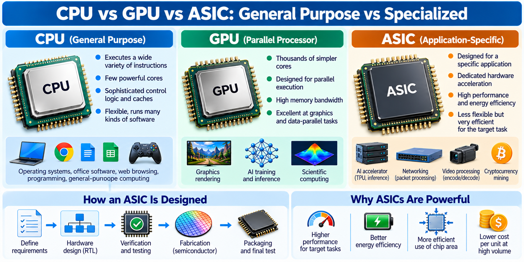
Unlike a general-purpose CPU, which executes many different kinds of software, an ASIC is optimized to perform specific operations efficiently.
ASICs are widely used in smartphones, networking equipment, artificial intelligence accelerators, video processing systems, automobiles, and industrial electronics.
For example, an ASIC designed for video processing may contain specialized circuits that encode or decode video efficiently.
A networking ASIC may process and forward large numbers of data packets.
An AI accelerator may contain dedicated hardware for matrix multiplication and other neural network operations.
The main advantage of an ASIC is specialization.
Engineers can design hardware around the exact computational requirements of an application instead of relying entirely on general-purpose instruction execution.
This specialization can improve performance, reduce power consumption, and provide more efficient use of semiconductor area.
However, ASICs are expensive to develop and generally less flexible than programmable alternatives.
2. What Does ASIC Stand For?
ASIC stands for Application-Specific Integrated Circuit.
The term application-specific means that the chip is designed for a defined purpose rather than unrestricted general-purpose computing.
For example, a CPU is designed to execute a broad range of machine instructions. It can run operating systems, web browsers, databases, and many other applications.
An ASIC may implement selected operations directly in electronic circuits.
This reduces the need to execute long sequences of general-purpose instructions for those operations.
However, an ASIC is not necessarily completely fixed or incapable of running software.
Many ASICs include embedded CPU cores, memory, configuration registers, and firmware-controlled functions.
The term ASIC describes the chip’s specialized design objective, not the absence of programmability.
3. How Does an ASIC Work?
An ASIC works by using electronic circuits designed to implement particular functions.
Like other digital chips, an ASIC contains transistors, logic gates, registers, memory structures, and electrical interconnections.
The difference lies in how those components are organized.
For example, consider a chip designed to encrypt network data.
A general-purpose CPU can perform encryption using software instructions.
A dedicated cryptographic ASIC can implement selected encryption operations directly in hardware.
Data enters the chip through an interface, passes through specialized processing circuits, and produces the required output.
The hardware can be organized into pipelines that process multiple data blocks efficiently.
An ASIC may also contain controllers and memory buffers to coordinate operations.
The exact architecture depends on the application.
ASICs can therefore combine specialized processing circuits with programmable control functions.
4. Why Are ASICs So Powerful?
ASICs can be powerful because they eliminate some of the overhead associated with general-purpose computation.
A CPU must support many different instructions and software execution patterns.
Its hardware includes instruction decoding, scheduling, registers, caches, and other structures that provide flexibility.
An ASIC can devote more of its available transistor budget to the operations required by its intended workload.
For example, a matrix multiplication accelerator can contain many specialized multiply-accumulate units connected to an efficient data movement system.
Instead of repeatedly interpreting general-purpose instructions, the hardware performs the intended numerical operations through dedicated circuits.
This can improve computational throughput and energy efficiency.
However, the advantage depends on workload suitability.
An ASIC optimized for one function may perform poorly or be unable to execute unrelated tasks.
Specialization provides efficiency at the expense of flexibility.
5. What Is the Difference Between an ASIC and a CPU?
A CPU is designed for general-purpose instruction execution.
It can run many different software programs without changing its physical hardware.
An ASIC is designed around a specific application or class of operations.
For example, a CPU can execute software for encryption, video processing, networking, and artificial intelligence.
A specialized ASIC may accelerate one of these functions using dedicated circuitry.
The CPU offers greater flexibility.
The ASIC may provide better performance per watt or higher throughput for its target workload.
However, ASICs can contain embedded CPUs, and modern CPUs also include specialized hardware accelerators.
The categories are therefore not completely separate.
The important distinction is the overall design objective.
6. What Is the Difference Between an ASIC and a GPU?
A GPU is a programmable processor optimized for graphics and suitable parallel computation.
It contains many execution resources capable of performing different operations under software control.
An ASIC can be optimized more narrowly for particular computational patterns.
For example, a GPU may support graphics rendering, scientific simulations, AI training, and other parallel workloads.
A custom AI ASIC may focus primarily on matrix operations, specialized numerical formats, and efficient movement of neural network data.
For suitable workloads, the ASIC may achieve better energy efficiency or computational density.
However, the GPU typically provides broader programming flexibility and a more general parallel computing environment.
A specialized ASIC is not automatically faster than every GPU.
Actual performance depends on architecture, memory bandwidth, numerical precision, software, and workload characteristics.
7. What Is the Difference Between an ASIC and an FPGA?
An FPGA, or Field-Programmable Gate Array, contains configurable logic and programmable interconnections.
Engineers can configure an FPGA to implement different digital circuits after manufacturing.
An ASIC has its primary physical circuit structure determined during fabrication.
For example, engineers can implement a custom data-processing pipeline on an FPGA and modify the design during development.
Once the design is stable, a suitable ASIC implementation may offer better power efficiency, performance, or cost per unit at sufficient production volume.
However, ASIC development requires substantial engineering work and manufacturing investment.
An FPGA is often preferred for prototyping, research, lower-volume products, and applications requiring hardware reconfiguration.
An ASIC is attractive when the functionality is sufficiently stable and the development cost can be justified.
8. What Is the Difference Between an ASIC and an SoC?
An SoC, or System on a Chip, integrates multiple system functions into one semiconductor device.
An ASIC is designed for a particular application.
These concepts describe different aspects of chip design.
For example, a smartphone SoC may be a custom ASIC containing CPU cores, GPU hardware, memory controllers, image processing circuits, and AI accelerators.
A simple ASIC may contain only a specialized signal-processing circuit.
Therefore, an ASIC can be an SoC, but not every ASIC is a complete system-level design.
The term ASIC emphasizes specialization, while SoC emphasizes functional integration.
9. What Are Common Types of ASICs?
ASICs are used in many electronic applications.
Networking ASICs perform functions such as packet forwarding, traffic processing, and high-speed switching.
Cryptographic ASICs accelerate selected encryption, hashing, and security operations.
Video processing ASICs implement compression, decompression, and other media operations.
AI ASICs accelerate neural network computations.
Storage controller ASICs manage data movement and other functions in storage devices.
Industrial ASICs implement specialized control or signal-processing functions.
Some ASICs are designed for extremely high-volume products, while others serve specialized industrial markets.
The architecture is determined by the application’s performance, power, cost, and reliability requirements.
10. Why Are ASICs Important for Artificial Intelligence?
Artificial intelligence workloads often require large numbers of numerical operations.
Neural networks commonly use matrix multiplication and multiply-accumulate operations.
These operations can be implemented efficiently using specialized hardware.
An AI ASIC may contain matrix processing arrays, on-chip SRAM, dedicated data movement circuits, and high-bandwidth interfaces.
The objective is to keep the arithmetic hardware supplied with data while minimizing unnecessary memory transfers.
For example, repeatedly moving model parameters between external memory and processing units can consume substantial energy.
An ASIC can optimize data reuse and memory access for selected AI operations.
However, AI algorithms evolve, and an accelerator must support the operations and numerical formats required by its software ecosystem.
The best AI ASIC balances specialization with enough flexibility to remain useful across intended workloads.
11. What Is Google’s TPU?
TPU stands for Tensor Processing Unit.
Google’s TPUs are specialized processors developed to accelerate machine learning workloads.
They use architectures designed for numerical operations common in neural networks.
Different TPU generations provide different compute, memory, and communication capabilities.
TPUs are examples of application-specific AI accelerators.
Unlike general-purpose CPUs, their primary design objective is efficient machine learning computation.
However, TPU-based systems still depend on CPUs, memory, communication networks, and supporting software.
The TPU does not replace every other component of a computing system.
It accelerates the operations for which its architecture is designed.
12. What Is a Bitcoin Mining ASIC?
Bitcoin mining is another example of specialized ASIC computing.
Bitcoin uses SHA-256-based hashing within its proof-of-work mechanism.
Mining equipment repeatedly computes hashes while searching for results that satisfy the network’s difficulty target.
These computations are highly repetitive and can be implemented using dedicated hardware.
A Bitcoin mining ASIC is designed to perform this hashing workload efficiently.
Compared with general-purpose CPUs or GPUs, a specialized mining ASIC can provide much higher hashing throughput and better energy efficiency for its intended operation.
However, the device is extremely specialized.
It cannot simply be repurposed to run ordinary desktop applications or arbitrary GPU workloads.
This illustrates both the strength and limitation of ASIC design.
13. How Are ASICs Designed?
ASIC development begins with defining the required functions and performance targets.
Engineers determine what the chip must accomplish, how much power it can consume, and what interfaces it needs.
For digital ASICs, designers commonly use Verilog or SystemVerilog to describe hardware behavior.
The design may be represented at the Register Transfer Level, or RTL.
Simulation and formal verification techniques help confirm that the circuit behaves as intended.
Logic synthesis converts the RTL into a gate-level implementation using a semiconductor technology library.
Physical design tools then place the logic cells and create the required interconnections.
Engineers perform timing analysis, power analysis, and physical verification.
Once the design is finalized, manufacturing data is prepared for semiconductor fabrication.
The completed dies are tested, packaged, and validated.
This process is substantially more complex than compiling an ordinary software program.
14. What Is RTL in ASIC Design?
RTL stands for Register Transfer Level.
It is a hardware design abstraction describing how digital information moves between registers and how combinational logic processes that information.
For example, an ASIC designer may describe a counter, arithmetic unit, communication controller, or processing pipeline using RTL.
The RTL specifies the intended digital behavior.
It does not necessarily describe each transistor individually.
Synthesis tools convert suitable RTL into interconnected logic cells.
These cells are mapped to the chosen semiconductor manufacturing technology.
Physical design tools then arrange the cells and create wiring.
RTL is also used in FPGA development.
The difference is that FPGA implementation maps the design into existing configurable hardware, while ASIC implementation ultimately produces a manufactured semiconductor circuit.
15. What Is ASIC Verification?
Verification determines whether an ASIC design satisfies its functional requirements before manufacturing.
This is essential because correcting a design error after fabrication can be expensive.
Engineers use simulation to test circuit behavior under different input conditions.
Testbenches generate stimuli and check the design’s responses.
Formal verification can mathematically analyze selected properties of a design.
Other verification methods examine timing, interfaces, clock-domain crossings, reset behavior, and additional implementation concerns.
For example, a network processing ASIC must handle expected packet formats and control conditions correctly.
A failure in its logic may affect the entire product.
Verification is therefore one of the largest and most important parts of ASIC development.
16. How Are ASICs Manufactured?
After design and verification, the ASIC is manufactured using semiconductor fabrication processes.
The process begins with a silicon wafer.
Photolithography, deposition, etching, doping, and other operations create transistor structures.
Additional layers form electrical contacts and metal interconnections.
Many copies of the ASIC are fabricated across one wafer.
After fabrication, the wafer undergoes electrical testing.
The wafer is then separated into individual dies.
Usable dies are assembled into suitable packages and tested again.
Modern ASICs may use mature or advanced semiconductor processes depending on their requirements.
A specialized industrial ASIC may use an older process, while a high-performance AI accelerator may benefit from a leading-edge process.
The most advanced process is not automatically the most economical choice.
17. Why Is ASIC Development Expensive?
ASIC development involves substantial engineering and manufacturing costs.
Design teams must develop the architecture, digital logic, interfaces, verification environment, and physical implementation.
Electronic design automation tools and semiconductor intellectual property can also be expensive.
Manufacturing requires masks, wafer fabrication, packaging, and testing.
For advanced process technologies, mask and development costs can be particularly high.
These expenses are often called non-recurring engineering costs, or NRE.
NRE represents development expenses that are not repeated for every individual chip.
Once the ASIC enters high-volume production, the cost per unit may become attractive.
However, low production volumes may not justify the initial investment.
This is why FPGAs and standard processors are often preferred for prototypes and smaller projects.
18. Why Can ASICs Be Cheaper in Large Quantities?
ASICs may provide lower unit costs when manufactured in sufficiently large quantities.
A custom chip can integrate the required functions without including unnecessary programmable resources.
This can reduce silicon area, package complexity, or the need for external components.
However, the development investment must be recovered across the production volume.
For example, a project producing only a few hundred devices may find ASIC development uneconomical.
A product manufactured in millions of units may justify a custom design.
The actual economics depend on design complexity, process technology, die area, yield, packaging, testing, and production volume.
Therefore, ASICs are often economically attractive when the application is stable and expected production quantities are high.
19. What Are the Disadvantages of ASICs?
The main disadvantage of ASICs is reduced flexibility compared with general-purpose processors and reconfigurable hardware.
Once an ASIC is manufactured, its physical logic cannot normally be changed in the same way as an FPGA configuration.
Some ASICs support firmware updates and programmable control, but these cannot correct every possible hardware design error.
ASIC development also requires significant engineering expertise and verification.
Manufacturing costs can be high, particularly for advanced semiconductor processes.
Development schedules may be longer than those for software-only solutions or FPGA prototypes.
Another risk is changing application requirements.
If the intended workload changes significantly, a specialized ASIC may become less useful.
ASIC development therefore requires careful consideration of performance requirements, product lifetime, production volume, and future flexibility.
20. When Should Engineers Choose an ASIC?
An ASIC is attractive when an application requires specialized performance, low power consumption, compact hardware, or economical high-volume manufacturing.
For example, a company producing millions of identical electronic devices may benefit from integrating their required functions into one custom chip.
A data center may use specialized accelerators to improve performance per watt for particular computing workloads.
A networking equipment manufacturer may require dedicated hardware for packet processing at high data rates.
However, ASIC development is not always appropriate.
For early prototypes, rapidly changing requirements, or small production quantities, a CPU, MCU, GPU, or FPGA may be more practical.
The correct decision depends on technical requirements and economic considerations.
21. Can an ASIC Be Reprogrammed?
Some ASIC functions can be configured or controlled through software.
For example, an ASIC may contain configuration registers, embedded processors, or firmware-controlled subsystems.
A network ASIC may support programmable forwarding rules.
An AI ASIC may execute different supported neural network models.
However, the fundamental physical organization of the ASIC’s specialized circuits is established during manufacturing.
This differs from an FPGA, where configurable logic resources can be used to implement different digital hardware structures.
Therefore, the statement that ASICs cannot be programmed is too simplistic.
Many ASICs are software-programmable within the capabilities of their fixed hardware architecture.
The distinction is between programming supported behavior and physically reconfiguring the underlying logic implementation.
22. Where Are ASICs Used?
ASICs are used throughout modern electronics.
Smartphones contain specialized circuits for image processing, security, communication, and multimedia functions.
Network equipment uses ASICs for packet forwarding and high-speed data processing.
Data centers use specialized accelerators for artificial intelligence and other computational workloads.
Storage devices use controller ASICs to manage flash memory and data transfers.
Automobiles use specialized semiconductor devices for selected control, communication, and processing functions.
Consumer electronics use ASICs for video, audio, display, and other dedicated operations.
Industrial equipment may use custom chips for specialized signal processing and control.
ASIC technology is important because many electronic products require functions that can be implemented more efficiently through dedicated hardware than through general-purpose software alone.
23. Common Misunderstandings About ASICs
One common misunderstanding is that an ASIC is always faster than a CPU or GPU.
In reality, an ASIC is optimized for particular operations, and its advantages depend on the workload.
Another misconception is that ASICs cannot execute software.
Many ASICs contain programmable processors and configurable hardware functions.
Some people assume that an ASIC is simply a smaller CPU.
An ASIC may use a completely different architecture designed around its intended function.
Another misunderstanding is that every ASIC uses the newest semiconductor manufacturing process.
Many ASICs use mature processes because they provide suitable cost, reliability, and electrical characteristics.
It is also incorrect to assume that ASICs are always cheaper.
Their development costs can be substantial, and low-volume products may be more economical using standard processors or FPGAs.
Finally, an ASIC is not necessarily a single-function circuit. Complex ASICs can combine several related processing and control functions.
24. Conclusion: Why Are Custom ASIC Chips So Powerful?
An ASIC, or Application-Specific Integrated Circuit, is a semiconductor chip designed for a particular application or class of operations.
Unlike a general-purpose CPU, an ASIC can devote substantial hardware resources to the functions required by its target workload.
This specialization can reduce instruction-processing overhead, improve data movement efficiency, and provide higher computational throughput or better performance per watt.
ASICs are used in artificial intelligence, networking, cryptography, video processing, storage, communication, and industrial systems.
However, specialization also creates limitations.
ASICs require significant design and verification effort, can be expensive to manufacture initially, and generally provide less hardware flexibility than FPGAs.
They are most attractive when performance requirements are clear, the workload is stable, and the production volume or operational benefits justify the investment.
The most important principle is simple: a CPU is designed to perform many different tasks, while an ASIC is designed to perform selected tasks exceptionally efficiently through specialized hardware.
Understanding ASICs provides a foundation for learning custom chip design, Verilog, RTL, FPGA development, semiconductor manufacturing, AI accelerators, and modern computer architecture.