1. What Do 3nm, 5nm, and 7nm Mean?
When discussing modern computer processors, smartphones, GPUs, and semiconductor manufacturing, you will often encounter terms such as 7nm, 5nm, 4nm, and 3nm.
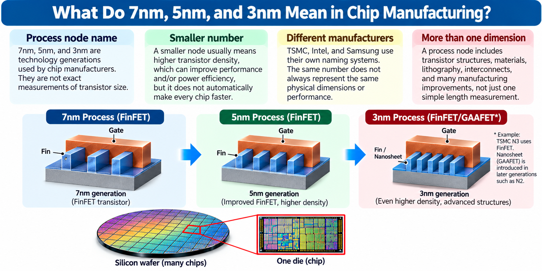
These numbers refer to semiconductor manufacturing technology generations, commonly called process nodes.
The abbreviation nm stands for nanometer. One nanometer is one-billionth of a meter.
However, an important distinction must be understood: in modern semiconductor manufacturing, a 3nm process does not mean that every transistor is exactly 3 nanometers long or wide.
Similarly, a 5nm processor does not necessarily contain transistors with a gate length of exactly 5 nanometers.
Modern process node names are technology labels used by semiconductor manufacturers to identify generations of manufacturing processes.
They represent combinations of transistor structures, manufacturing methods, material technologies, circuit density, performance characteristics, and power efficiency.
For example, TSMC uses names such as N7, N5, and N3 to identify different process technology families.
Intel uses names such as Intel 7, Intel 4, and Intel 3. Samsung also uses its own process technology designations.
These naming systems are not based on one universally standardized transistor measurement.
A newer process may allow engineers to integrate more transistors into a given area, improve transistor performance, reduce power consumption, or achieve a combination of these benefits.
However, a smaller node number does not automatically guarantee that every chip manufactured using that process will be faster or more energy-efficient.
Understanding these distinctions is essential for comparing modern processors and learning how semiconductor technology develops.
2. What Is a Nanometer?
A nanometer is a unit of length in the metric system.
One nanometer equals 0.000000001 meter, or 10 to the power of minus nine meters.
There are one million nanometers in one millimeter.
To understand this scale, consider that a typical human hair has a diameter measured in tens of thousands of nanometers, although the exact diameter varies considerably.
Semiconductor manufacturing involves structures whose dimensions may be measured in nanometers.
These include transistor features, insulating layers, conductive structures, and other microscopic elements.
However, not every feature inside a modern integrated circuit is only a few nanometers in size.
Some components are much larger, including certain metal interconnections, analog devices, I/O structures, and power-related circuits.
Furthermore, a semiconductor process node name should not be interpreted as an exact measurement of every physical feature.
The nanometer remains a real scientific unit. What has changed is how semiconductor manufacturers use nanometer-related labels to name process technology generations.
3. What Is a Semiconductor Process Node?
A semiconductor process node describes a generation or family of manufacturing technology used to fabricate integrated circuits.
A process technology includes many engineering components.
These include transistor structures, material properties, manufacturing sequences, lithography techniques, design rules, metal interconnections, and available circuit libraries.
For example, a manufacturer may offer a process optimized for high-performance processors and another variation optimized for low-power devices.
Both variations may belong to the same general node family.
The process node affects how chip designers implement their circuits.
A new node may provide smaller standard cells, different transistor electrical characteristics, more advanced interconnections, or improved manufacturing capabilities.
However, the node name does not fully describe the manufacturing technology.
Two processes with the same nominal node label may differ in transistor density, power consumption, performance, and manufacturing cost.
The process node should therefore be understood as a technology classification rather than a single physical dimension.
4. Why Did Process Nodes Originally Use Physical Dimensions?
Earlier semiconductor technology generations were more closely associated with measurable features of transistors or manufacturing patterns.
For example, older process generations were often described using dimensions associated with transistor gate lengths or other important structures.
As semiconductor manufacturing advanced, these physical dimensions became smaller.
Process technology names such as 350nm, 250nm, 180nm, and 130nm reflected this historical approach.
However, semiconductor devices became increasingly complex.
Different parts of a transistor did not necessarily shrink by the same proportion.
The dimensions of gates, contacts, wiring, and other structures began following different scaling patterns.
Manufacturers also introduced new transistor designs, materials, and circuit techniques.
As a result, the relationship between a process node name and one physical dimension became less direct.
The semiconductor industry eventually moved toward using node names primarily as generation identifiers.
This is why a modern 3nm process cannot be understood simply by imagining a transistor with a 3nm gate.
5. Does 3nm Mean a Transistor Is 3 Nanometers Wide?
No. A 3nm process name does not specify that every transistor has a width of 3 nanometers.
A transistor has multiple physical dimensions.
These may include gate length, channel width, gate pitch, contact spacing, and other features.
For a FinFET transistor, the fin structure introduces additional dimensions.
For a gate-all-around transistor, nanosheet width, thickness, spacing, and gate geometry become important.
These dimensions are not all equal.
Furthermore, many transistor characteristics are determined by three-dimensional structures rather than a single length.
For example, a transistor’s effective channel width can depend on the geometry of multiple fins or nanosheets.
A modern process node represents an overall manufacturing platform.
Therefore, the statement that a processor uses 3nm technology does not tell us the exact dimensions of all its transistors.
To understand the physical structures, engineers examine detailed process information rather than relying on the node label alone.
6. What Is Transistor Gate Length?
Gate length is one of the important physical dimensions associated with a MOSFET.
A MOSFET controls electrical conduction through a semiconductor channel using an electric field generated by its gate.
In a simplified planar transistor, gate length refers to the physical dimension of the gate along the direction of current flow through the channel.
Gate length influences transistor behavior, including switching characteristics and electrostatic control.
However, transistor operation depends on many other parameters.
These include channel geometry, doping, dielectric materials, source and drain structures, applied voltages, and parasitic effects.
In advanced semiconductor technologies, physical gate length and effective channel length may not be identical.
Modern transistor structures are also more complicated than the traditional planar MOSFET model.
This is one reason process node labels no longer provide a reliable direct measurement of transistor gate length.
7. What Is Transistor Pitch?
Pitch is the distance between corresponding features in a repeating physical pattern.
In semiconductor manufacturing, engineers use several pitch measurements.
One example is contacted gate pitch, which describes the spacing between adjacent contacted transistor gate structures under a particular layout definition.
Another is metal pitch, which describes the spacing between neighboring metal routing lines.
These measurements influence how densely circuits and their connections can be arranged.
Smaller pitches may allow greater integration density, but the relationship is not automatic.
Circuit area also depends on transistor architecture, cell design, contact placement, routing resources, and other constraints.
Two semiconductor processes may have different gate and metal pitches even when their marketing labels appear similar.
For meaningful technical comparisons, physical pitch measurements can provide more information than process node names alone.
However, no single pitch value completely describes the density or performance of a process.
8. What Is Transistor Density?
Transistor density describes how many transistors can be integrated into a particular area.
It is often expressed as millions of transistors per square millimeter.
For example, if a hypothetical circuit contains 100 million transistors within an area of one square millimeter, the average density would be 100 million transistors per square millimeter.
However, actual density depends heavily on the circuit structure.
An SRAM array has a highly regular layout.
A processor core contains more varied logic structures and interconnections.
Analog and I/O circuits may require larger physical devices or wider spacing.
Therefore, transistor density is not uniform across a processor die.
Manufacturers sometimes publish density improvements using selected logic libraries or representative circuit structures.
These comparisons can be useful, but they should not automatically be interpreted as the density of every completed chip.
The actual density of a finished processor depends on its architecture and physical implementation.
9. Why Is Higher Transistor Density Important?
Higher transistor density allows more electronic functionality to be integrated into a limited semiconductor area.
For example, a processor designer may use the additional density to include more CPU cores, larger caches, or specialized accelerators.
Alternatively, the designer may reduce die area while maintaining similar functionality.
A smaller die can potentially increase the number of candidate dies produced on each wafer.
This may improve manufacturing economics when yield and other costs are favorable.
However, increased density also creates engineering challenges.
More active circuitry in a limited area can increase power density and complicate cooling.
Dense routing can create electrical interference, resistance, capacitance, and timing problems.
Therefore, improving transistor density is valuable, but it must be balanced against performance, power, thermal behavior, and manufacturing requirements.
10. What Is 7nm Chip Manufacturing?
7nm refers to a generation of advanced semiconductor manufacturing technology.
It became particularly important for high-performance processors and mobile chips during the late 2010s.
For example, TSMC began volume production of its N7 FinFET technology in 2018.
The technology provided improvements in transistor density, performance, and power characteristics compared with earlier generations.
The N7 process uses FinFET transistor structures.
A FinFET contains a raised semiconductor fin controlled by a gate that extends around multiple sides of the channel.
This structure provides improved electrostatic control compared with conventional planar transistor designs.
An important technical distinction is that TSMC’s original N7 process did not require EUV lithography for its initial production implementation.
A related process, N7+, introduced EUV lithography for selected layers.
This illustrates that process technology development involves more than changing the node number.
Different variations within one generation may use different manufacturing methods.
11. What Is 5nm Chip Manufacturing?
5nm refers to a newer semiconductor process generation than 7nm within a manufacturer’s technology roadmap.
For example, TSMC introduced its N5 technology into volume production in 2020.
N5 continued using FinFET transistor technology while incorporating manufacturing improvements and extensive use of advanced patterning techniques.
EUV lithography became increasingly important in this generation.
Compared with the company’s N7 technology, N5 offered improvements in logic density, performance, and power efficiency.
However, these improvements should not be interpreted as universal percentages that apply to every finished processor.
The actual benefits depend on how a particular chip is designed and operated.
For example, a processor designer might use the additional transistor density to increase cache capacity.
Another designer might prioritize lower power consumption.
A third designer might aim for higher computational throughput.
The same semiconductor process can support different architectural decisions.
12. What Is 3nm Chip Manufacturing?
3nm refers to another advanced semiconductor manufacturing generation.
For example, TSMC introduced its N3 technology into high-volume production in 2022.
An important fact is that TSMC’s original N3 technology continued using FinFET transistors.
The name 3nm did not automatically mean that the manufacturing process switched to gate-all-around transistors.
TSMC developed several variants within its N3 family, including technologies optimized for different power, performance, density, and product requirements.
The N3 family offers improvements over earlier generations through process optimization, circuit design capabilities, and manufacturing advances.
However, a 3nm process is not simply a 5nm process with every transistor dimension reduced to three-fifths of its previous size.
Different features scale differently, and some structures may not become smaller at all.
The process represents a complete technology platform.
This is why comparing 3nm and 5nm requires examining actual density, performance, power, and cost characteristics.
13. What Is the Difference Between 7nm, 5nm, and 3nm?
The most important difference is that these labels identify different semiconductor process generations within a manufacturer’s technology family.
A newer process generation may introduce improvements in transistor structures, fabrication methods, circuit density, or electrical characteristics.
For example, in TSMC’s process development, N7 was followed by N5 and then N3 as successive major technology generations.
N5 introduced significant scaling and manufacturing improvements over N7.
N3 provided further advances while retaining FinFET technology.
However, the process labels should not be compared using the simple calculation 7 divided by 5 or 5 divided by 3.
A reduction in the node number does not imply an identical proportional reduction in transistor dimensions.
Nor does it imply a proportional increase in CPU frequency.
The proper comparison depends on the specific foundry process and its published technical characteristics.
14. Does 3nm Have More Transistors Than 5nm?
A 3nm-class process may provide higher transistor density than a previous 5nm-class process from the same manufacturer.
However, this does not mean every 3nm chip contains more transistors than every 5nm chip.
A chip designer decides how much functionality to implement.
For example, a relatively small processor manufactured using 3nm technology may contain fewer transistors than a large GPU manufactured using 5nm technology.
The GPU could have a much larger die and more total circuitry.
Transistor count depends on the chip design.
Transistor density depends on the semiconductor process and physical implementation.
These are related but different concepts.
A newer process may allow more transistors to fit within the same area, but the manufacturer is not required to use all that potential density.
15. Does 3nm Make a Processor Faster?
Not automatically.
A newer semiconductor process may provide transistors with improved electrical characteristics.
These improvements can create opportunities for higher performance.
However, processor speed depends on more than transistor technology.
CPU performance is influenced by instruction throughput, execution architecture, cache design, branch prediction, memory latency, operating frequency, and software behavior.
For example, a processor with a more efficient architecture may perform better than another processor manufactured using a newer process.
Thermal and power limits also matter.
A chip may contain transistors capable of operating at higher speeds but still be limited by its power budget.
Therefore, the process node is one factor in performance, not a complete performance measurement.
The best way to compare processors is to examine their architecture, specifications, and measured performance in relevant applications.
16. Does 3nm Use Less Power Than 5nm?
A newer process can provide opportunities for reducing power consumption.
For example, improved transistor characteristics may allow certain circuits to operate at lower voltage or achieve the same performance with less energy.
However, total processor power depends on operating voltage, frequency, switching activity, leakage current, architecture, and workload.
A simplified expression for dynamic CMOS power is:
P ≈ αCV²f
In this equation, P represents dynamic power, α represents switching activity, C represents effective switched capacitance, V represents supply voltage, and f represents switching frequency.
This relationship explains why voltage and circuit activity are important.
A newer process might reduce capacitance or support lower operating voltage.
However, the designer may instead use the technology to increase operating frequency or add more functional units.
Consequently, a high-performance 3nm processor can consume more total power than a lower-performance 5nm processor.
Power efficiency must be evaluated under comparable operating conditions.
17. What Does Performance per Watt Mean?
Performance per watt is a measure of how much computational work a processor can perform for a given amount of electrical power.
It is especially important for smartphones, laptops, servers, and AI accelerators.
For example, two processors may provide similar performance while consuming different amounts of energy.
The processor requiring less electrical power is more energy-efficient for that particular workload.
Alternatively, two processors may consume similar power while one completes more work.
Again, the processor completing more useful work has better performance per watt for that workload.
New semiconductor process technologies can improve performance per watt.
However, architectural improvements also play a major role.
A better cache design, specialized arithmetic unit, or reduced data movement can improve energy efficiency even without moving to a new process node.
Therefore, semiconductor technology and computer architecture must be evaluated together.
18. What Is PPA in Semiconductor Design?
PPA stands for Power, Performance, and Area.
These are three central considerations in integrated circuit design.
Power refers to the electrical energy consumed by the circuit during operation.
Performance refers to how effectively the circuit completes its intended work, including relevant timing or throughput requirements.
Area refers to the physical semiconductor space occupied by the implementation.
Engineers often face trade-offs among these objectives.
For example, a faster circuit may require larger transistors or additional hardware.
A more compact implementation may create timing or routing challenges.
A low-power design may operate at a lower frequency.
Semiconductor process improvements can expand the available design options, but no process automatically optimizes every objective simultaneously.
For this reason, foundries and chip designers frequently discuss PPA when comparing manufacturing technologies.
19. What Is a FinFET Transistor?
FinFET stands for Fin Field-Effect Transistor.
It is a semiconductor transistor structure developed to improve electrostatic control over the conductive channel.
In a traditional planar MOSFET, the channel is relatively flat.
A FinFET uses a raised fin-shaped semiconductor channel.
The gate controls the channel from multiple sides.
This geometry helps reduce certain short-channel effects and improves control over leakage current.
FinFETs became important in advanced semiconductor manufacturing as traditional planar structures encountered scaling limitations.
TSMC’s N7, N5, and original N3 technologies are examples of FinFET-based process generations.
However, using FinFET technology does not mean that every transistor is identical across these processes.
Fin dimensions, gate structures, materials, contacts, and interconnect characteristics can vary significantly.
20. What Is a GAAFET Transistor?
GAAFET stands for Gate-All-Around Field-Effect Transistor.
A GAAFET uses a gate structure that surrounds the conductive channel more completely than in a conventional FinFET.
Some implementations use nanosheets or nanowires.
The goal is to improve electrostatic control over the channel.
This can help reduce certain leakage problems and provide additional opportunities for device scaling.
However, manufacturing GAAFET structures is complex.
The process requires precise control over channel geometry, gate materials, insulating layers, and contacts.
An important distinction is that GAAFET adoption does not correspond to one universal node number across every manufacturer.
For example, TSMC retained FinFETs in its N3 family and introduced nanosheet transistors in its N2 generation.
Different foundries can adopt transistor architectures at different points in their technology roadmaps.
Therefore, a process node label alone does not reveal whether the transistors are FinFETs or GAAFETs.
21. Why Did the Semiconductor Industry Move Beyond Planar Transistors?
As transistors became smaller, maintaining electrical control over their channels became increasingly difficult.
One challenge involves leakage current when a transistor is supposed to be off.
Another involves short-channel effects, where the source and drain structures influence channel behavior in unwanted ways.
Smaller physical dimensions can also increase sensitivity to manufacturing variations.
FinFET technology improved channel control through a three-dimensional structure.
GAAFET technology provides another approach by surrounding the channel more completely with the gate.
These changes demonstrate that process scaling is not simply a matter of shrinking a two-dimensional drawing.
Engineers must redesign device structures to maintain suitable electrical behavior at increasingly demanding scales.
22. What Is EUV Lithography?
EUV stands for Extreme Ultraviolet.
EUV lithography is an advanced patterning technology used in semiconductor manufacturing.
It operates using light with a wavelength of approximately 13.5 nanometers.
This is much shorter than the 193-nanometer wavelength used in advanced deep ultraviolet lithography systems.
The shorter wavelength helps manufacturers pattern certain fine features with suitable optical and process techniques.
However, EUV lithography is not a simple photographic printing process.
EUV radiation is strongly absorbed by many materials.
Therefore, EUV systems use specialized reflective optics and vacuum environments.
The systems require complex light sources, precision mirrors, wafer positioning mechanisms, and contamination control.
EUV is particularly important for selected critical layers in advanced semiconductor manufacturing.
However, not every layer of a modern 3nm or 5nm chip is patterned using EUV.
Manufacturers choose appropriate lithography techniques for different process layers.
23. Does EUV Mean the Transistors Are 13.5nm?
No. The 13.5nm number refers to the wavelength of the EUV light used in lithography.
It does not directly represent the size of the finished transistor.
Similarly, the use of 193nm DUV light does not mean that the smallest manufactured features must be 193 nanometers wide.
Modern lithography uses complex optical techniques, process optimization, and sometimes multiple-patterning approaches.
The relationship between exposure wavelength and final feature dimensions is influenced by the optical system, patterning strategy, and manufacturing process.
EUV technology helps improve the ability to manufacture fine features.
However, the process node name, exposure wavelength, gate length, and metal pitch describe different technical quantities.
These values should not be confused with one another.
24. Why Is 3nm Manufacturing More Difficult?
Advanced semiconductor manufacturing requires extremely precise process control.
As certain circuit dimensions become smaller, manufacturing variations and defects can have increasingly significant consequences.
Lithography must define complex patterns with tight overlay requirements.
Etching must create carefully controlled structures.
Deposition must produce thin material layers with suitable properties.
Transistor formation requires sophisticated materials and device geometries.
Interconnect resistance, capacitance, and power delivery also become major challenges.
Manufacturers must inspect and measure structures throughout fabrication.
The production process involves a large number of carefully coordinated steps.
Improving yield while maintaining electrical performance requires extensive engineering work.
The complexity of advanced manufacturing is one reason leading-edge semiconductor fabrication demands substantial equipment investment, research, and process development.
25. What Is Semiconductor Yield?
Yield describes the proportion of manufactured devices that satisfy the required acceptance criteria.
For example, if a wafer contains 100 candidate dies and 85 meet the relevant test requirements, the simplified die yield is 85 percent.
Actual yield analysis is more complicated because semiconductor defects and variations can affect different parts of a circuit.
Yield depends on factors such as defect density, process stability, die size, circuit design, and testing criteria.
When a new manufacturing process is introduced, engineers work to improve its yield.
A process with attractive transistor performance but poor manufacturing yield may be expensive to use.
Over time, manufacturing experience and process optimization can improve production results.
Yield is therefore an essential part of the economic value of a semiconductor process.
A process node should not be evaluated only by its transistor dimensions or nominal performance.
26. Why Are Advanced Process Nodes More Expensive?
Advanced process nodes generally require complex manufacturing techniques and substantial development investment.
Lithography equipment, precision deposition systems, etching tools, inspection equipment, and other machinery are expensive.
Advanced photomasks can also contribute significantly to development costs.
The design process becomes more demanding as engineers work with increasingly complex manufacturing rules.
Physical design tools must account for routing constraints, timing behavior, power delivery, and other effects.
Testing and verification requirements can also increase.
Additionally, yield influences the effective cost per acceptable die.
A smaller process may allow more transistors per unit area, but the cost of manufacturing each wafer may also increase.
Therefore, moving to a newer node does not guarantee that every chip becomes cheaper to produce.
The economic result depends on process cost, die area, yield, design investment, packaging, and production volume.
27. Does a Smaller Node Always Mean a Smaller Die?
No. A newer process may provide greater transistor density, but the final die size depends on the chip design.
For example, a manufacturer may use additional density to include more processor cores.
Another manufacturer may increase cache capacity.
A third may integrate a larger GPU or AI accelerator.
These changes can consume the area savings offered by the newer process.
Furthermore, not every circuit structure scales at the same rate.
SRAM cells, analog components, I/O circuits, and high-current structures may have different scaling limitations.
The completed die may therefore remain the same size or even become larger.
The process node provides additional design opportunities, but the chip architect determines how those opportunities are used.
28. Why Does SRAM Not Always Scale Like Logic?
SRAM stands for Static Random Access Memory.
It is widely used for processor caches and other high-speed storage structures.
A typical SRAM cell uses six transistors to maintain one stored bit while power is supplied.
SRAM arrays have regular layouts and strict requirements involving stability, access time, and electrical behavior.
As semiconductor processes advance, logic circuits and SRAM cells may experience different density improvements.
Certain transistor scaling techniques that benefit standard logic do not necessarily reduce SRAM cell area by the same proportion.
This is important because modern processors often dedicate substantial die area to cache memory.
For example, a process might provide a large improvement in logic density but a smaller improvement in SRAM density.
Consequently, the overall die-area reduction depends on how much of the chip consists of logic, SRAM, analog circuits, and other structures.
This is another reason node numbers cannot be translated directly into whole-chip area reductions.
29. Why Do Analog and I/O Circuits Scale Differently?
Modern processors contain more than digital logic.
They may include analog circuits, clock generation structures, memory interfaces, high-speed communication transceivers, and other components.
These circuits have electrical requirements that differ from ordinary logic gates.
For example, an I/O circuit may need to tolerate a particular voltage range.
An analog amplifier may require transistor characteristics optimized for noise, gain, or matching.
Some components also depend on physical capacitance, resistance, or high-voltage spacing requirements.
Reducing every dimension may not improve their performance.
Therefore, advanced process technologies may provide specialized devices or design options for these functions.
In some products, manufacturers place certain I/O functions on separate dies manufactured using a more mature process.
This is one reason chiplet architectures have become attractive for selected semiconductor systems.
30. Can We Compare TSMC, Intel, and Samsung by Node Number?
Not reliably using the node number alone.
TSMC, Intel, and Samsung develop different semiconductor process technologies.
Each company has its own manufacturing methods, transistor designs, design rules, and naming conventions.
For example, Intel 7 and TSMC N7 are not guaranteed to have identical density or electrical characteristics merely because both names contain the number seven.
Likewise, TSMC N3 and another manufacturer’s 3nm-class process should not be assumed to use the same transistor structure.
Meaningful comparisons require examining technical information such as logic density, transistor performance, power efficiency, interconnect characteristics, yield, and cost.
Even these measurements must be compared under suitable conditions.
For example, one manufacturer’s density claim may use a different representative logic structure from another manufacturer’s claim.
The most reliable comparison examines actual processes and their characteristics rather than treating node labels as universal physical dimensions.
31. Why Did Intel Change Its Process Node Naming?
Intel revised its process naming system in 2021 to align its terminology more closely with how advanced semiconductor technologies were being described across the industry.
Its updated naming system includes names such as Intel 7, Intel 4, and Intel 3.
Intel has explicitly explained that modern process node names no longer correspond directly to one physical transistor dimension.
The company also emphasizes power, performance, and area when describing its manufacturing generations.
For example, Intel 4 introduced significant manufacturing and efficiency improvements over Intel 7 and made extensive use of EUV lithography.
However, it is incorrect to conclude that Intel 4 has a universal physical dimension of exactly 4 nanometers.
Intel’s naming system illustrates the broader semiconductor industry trend toward technology generation labels.
32. What Are N3E, N3P, N5P, and Other Process Variants?
Semiconductor foundries often offer several versions of one process technology family.
For example, TSMC has developed variations of its N3 and N5 families.
Different variants may emphasize performance, power efficiency, density, manufacturing cost, or compatibility with existing designs.
A process intended for a high-performance server processor may prioritize different electrical characteristics from one intended for a battery-powered mobile device.
Some variants improve an existing process without introducing an entirely new technology generation.
Others offer changes in transistor characteristics or circuit design capabilities.
These variations demonstrate that a process node is not one fixed manufacturing recipe.
The exact process variant matters when evaluating chip specifications.
Simply saying that a product is manufactured using 3nm technology may not identify the complete process configuration.
33. What Is the Difference Between 4nm and 5nm?
The distinction between 4nm and 5nm depends on the manufacturer.
For example, TSMC’s N4 technology is part of an enhanced manufacturing family related to its N5 generation.
It provides improvements while retaining important design compatibility characteristics.
Therefore, 4nm should not automatically be interpreted as a completely independent technology generation positioned at an exact physical midpoint between 5nm and 3nm.
A manufacturer may introduce an intermediate process to improve performance, power consumption, density, or manufacturing economics.
Process names are chosen within the company’s technology roadmap.
The actual engineering improvements must be evaluated through process specifications.
34. What Is 2nm Chip Manufacturing?
2nm is another advanced process technology generation label.
Like 3nm and 5nm, it should not be interpreted as a statement that every transistor feature measures exactly two nanometers.
The term identifies a newer manufacturing technology family.
For example, TSMC’s N2 generation introduces nanosheet transistor technology.
This represents a significant device architecture change relative to TSMC’s FinFET-based N3 family.
Nanosheet transistors use a gate-all-around structure intended to improve electrostatic control.
However, transistor architecture is only one part of the technology.
Manufacturing methods, interconnections, power delivery, circuit libraries, and design rules also determine the capabilities of the process.
The transition to newer process generations therefore involves complex engineering rather than a simple reduction in one measurement.
35. What Is an Angstrom in Semiconductor Manufacturing?
An angstrom is a unit of length equal to one-tenth of a nanometer.
One angstrom equals 0.1 nanometer.
In physical science, angstroms are often used to describe atomic-scale distances.
Some semiconductor process names use angstrom-related terminology.
However, these names should not automatically be interpreted as literal feature dimensions.
For example, a process label using an angstrom-related designation does not necessarily specify the exact transistor gate length.
The same naming caution applies as with nanometer-based process labels.
A modern manufacturing node name identifies a technology generation.
Understanding the angstrom unit is useful, but process technology comparisons still require detailed physical and electrical information.
36. What Is Backside Power Delivery?
Power delivery is an important challenge in modern integrated circuits.
A processor requires electrical power to be distributed to an enormous number of transistors.
Traditional advanced chips generally use metal interconnection structures above the transistor devices for both signal routing and power distribution.
As circuits become denser, competition for routing space can become increasingly difficult.
Backside power delivery is an approach that provides selected power connections through structures associated with the backside of the semiconductor die.
This can help separate some power delivery resources from frontside signal routing.
Potential advantages include improved routing flexibility and reduced power distribution limitations in suitable designs.
However, implementing backside power delivery requires additional manufacturing and design complexity.
It is not automatically included in every process with a smaller node number.
Backside power delivery illustrates how semiconductor improvements increasingly involve architecture and interconnection technology, not only transistor scaling.
37. Why Is Interconnect Technology So Important?
Transistors are only useful when they can communicate with other parts of the circuit.
Modern chips contain complex networks of metal interconnections.
These connections carry data, clock signals, and electrical power.
As semiconductor structures become denser, interconnect resistance and capacitance can become major performance limitations.
A transistor may switch quickly, but a long or heavily loaded connection can delay the signal reaching the next circuit.
Power distribution also becomes challenging when many transistors operate simultaneously.
Engineers therefore optimize metal layers, routing structures, contact resistance, and other physical features.
Some process improvements target interconnection technology rather than transistor dimensions alone.
The overall performance of a semiconductor process depends on the combined behavior of devices and wiring.
38. Why Can’t Semiconductor Manufacturers Keep Shrinking Transistors Forever?
Transistor scaling faces several physical and engineering limits.
As certain dimensions become smaller, controlling electrical behavior becomes more challenging.
Leakage current may increase.
Quantum mechanical tunneling can become important through sufficiently thin barriers.
Small manufacturing variations can have significant effects on device characteristics.
Electrical interconnections can introduce substantial resistance and delay.
Power density and heat removal also create limitations.
In addition, advanced manufacturing becomes increasingly expensive and complex.
These challenges do not mean semiconductor development must stop.
Instead, engineers pursue multiple improvement methods.
These include advanced transistor structures, improved materials, new interconnect designs, specialized accelerators, chiplets, three-dimensional integration, and advanced packaging.
Modern semiconductor progress therefore depends on more than conventional geometric scaling.
39. Why Are Older Process Nodes Still Used?
Not every semiconductor product requires the newest process.
Many useful electronic devices are manufactured using mature technologies such as 180nm, 130nm, 90nm, 65nm, 40nm, or 28nm.
For example, microcontrollers, analog interfaces, power management devices, industrial controllers, and automotive components may be manufactured using mature processes.
These products can have different requirements from high-performance CPUs or GPUs.
An industrial controller may prioritize reliability, temperature tolerance, long-term supply availability, and cost.
A power device may require high-voltage capabilities that are not well suited to a leading-edge logic process.
A small microcontroller may not benefit economically from an expensive advanced node.
Mature processes also have established manufacturing experience and often well-understood reliability characteristics.
Therefore, older semiconductor nodes remain important parts of the industry.
A smaller node number is not automatically better for every application.
40. What Does a Process Node Mean for Microcontrollers?
Microcontrollers are designed for embedded control applications.
They typically combine a CPU core, memory, timers, communication interfaces, and other peripherals.
Many microcontrollers operate at modest frequencies and have strict cost or power requirements.
For example, a microcontroller controlling a household appliance may not need billions of transistors or extremely dense digital logic.
A mature semiconductor process may provide sufficient performance while supporting integrated flash memory, analog interfaces, or other useful features.
Moving such a design to a newer process can introduce additional development costs and technical complications.
Therefore, microcontroller designers choose manufacturing processes based on actual requirements.
For many embedded applications, software support, peripherals, power consumption, reliability, and cost matter more than a leading-edge process label.
41. What Does a Process Node Mean for GPUs?
GPUs are large integrated circuits designed for high-throughput graphics and parallel computation.
Modern GPUs may contain substantial numbers of arithmetic units, registers, caches, and specialized acceleration circuits.
Advanced semiconductor processes can allow more computing resources to fit within a given die area.
They can also offer improvements in performance and energy efficiency.
However, GPU performance depends on architecture, memory bandwidth, cache design, clock frequency, software, and power limits.
For example, a GPU manufactured using a newer process may still perform worse than an older high-end GPU with substantially more execution resources.
Memory capacity and bandwidth can also be major limitations.
Therefore, the GPU’s process node should be evaluated alongside its complete hardware architecture.
42. What Does a Process Node Mean for AI Accelerators?
AI accelerators are designed to perform large quantities of numerical computation.
They frequently contain specialized matrix processing hardware, on-chip memory, control logic, and high-speed communication interfaces.
Advanced semiconductor processes can help integrate additional compute resources and improve energy efficiency.
However, AI performance is not determined solely by transistor density.
Large AI models require substantial memory capacity and bandwidth.
Moving data between processing units and memory can consume significant energy.
For some workloads, memory bandwidth is more important than peak arithmetic throughput.
Advanced packaging and high-bandwidth memory may therefore provide major benefits even when transistor scaling alone offers limited improvement.
AI accelerator design illustrates the importance of optimizing the complete system rather than focusing only on the process node.
43. Does a Smaller Node Improve Battery Life?
A more advanced manufacturing process can help improve the energy efficiency of a mobile processor.
This may contribute to longer battery life.
However, battery life depends on the entire device.
For example, a smartphone consumes power through its display, wireless communication systems, memory, storage, sensors, and other components.
The operating system and applications also affect how much work the processor performs.
A newer processor may provide better performance per watt, but software behavior and device design determine whether that improvement produces longer battery life.
A processor that completes tasks more quickly may be able to return to low-power states sooner.
However, demanding applications may use the additional performance to perform more work.
Therefore, process node improvements create opportunities for better battery life, but they do not guarantee a particular increase.
44. Does a Smaller Node Improve Gaming Performance?
Gaming performance depends on several components.
These include CPU performance, GPU performance, memory bandwidth, software optimization, and thermal conditions.
A newer semiconductor process may allow a CPU or GPU to operate more efficiently.
However, gaming performance also depends on architectural improvements and workload characteristics.
For example, one game may be limited by CPU performance, while another may be limited by GPU rendering capacity.
Increasing cache size or improving graphics execution architecture may provide substantial benefits.
A newer process node can support these improvements, but the node label alone does not predict gaming frame rates.
The correct comparison requires evaluating complete products under similar testing conditions.
45. Why Are Process Node Comparisons Often Misleading?
Process node labels are convenient because they provide short names for complex technologies.
However, they can encourage oversimplified comparisons.
For example, a reader may assume that 3nm must be 40 percent smaller than 5nm because the numerical label decreased from five to three.
This is not a valid semiconductor scaling calculation.
The physical dimensions of transistor features do not all scale according to the node name.
Another misleading assumption is that a 3nm CPU must outperform a 5nm CPU.
Performance depends on architecture and operating conditions.
A third mistake is comparing node labels from different manufacturers as though they followed one standardized measurement system.
The semiconductor industry has no universal rule requiring all manufacturers to assign the same node number to processes with identical physical characteristics.
To make meaningful comparisons, examine real technical measurements rather than relying only on the marketing label.
46. How Should You Compare Two Semiconductor Processes?
A useful semiconductor process comparison considers several technical characteristics.
First, examine transistor density using comparable definitions and circuit structures.
Second, compare transistor performance under appropriate operating conditions.
Third, evaluate power consumption or energy efficiency.
Fourth, review interconnect characteristics, including relevant resistance and routing capabilities.
Fifth, consider the types of transistors and devices supported by the technology.
Sixth, examine manufacturing maturity, yield, and cost.
For completed processors, architecture and workload-specific performance must also be considered.
For example, a process may provide excellent logic density but relatively modest SRAM scaling.
Another process may emphasize high operating frequency at the cost of increased power.
There is no single measurement that captures every advantage of a semiconductor manufacturing technology.
47. What Is the Difference Between Process Node and Processor Architecture?
The process node describes the manufacturing technology used to fabricate the chip.
Processor architecture describes how the processor is organized to perform computation.
For example, a CPU architecture may define its instruction execution pipeline, cache hierarchy, arithmetic units, and memory behavior.
The instruction set architecture defines the instructions visible to software.
Examples include x86, Arm, and RISC-V.
The process technology determines how the electronic circuits are physically implemented.
Two processors can use the same instruction set while being manufactured with different process technologies.
They can also have different microarchitectures even when manufactured using the same process.
Therefore, architecture and manufacturing technology are separate dimensions of processor design.
Both influence performance and power efficiency.
48. Can a 7nm Processor Be Better Than a 3nm Processor?
Yes, depending on the application and the specific products being compared.
For example, a large high-performance processor manufactured using a 7nm-class process may outperform a small low-power processor manufactured using a 3nm-class process in certain workloads.
The older processor may contain more cores, larger caches, or other resources.
It may also operate with a much larger power budget.
Conversely, the newer processor may provide better energy efficiency or stronger performance within a limited thermal envelope.
The result depends on the workload.
This is why CPU and GPU comparisons should use application benchmarks and complete hardware specifications rather than process node names alone.
A manufacturing node is not a substitute for performance measurement.
49. Does Moving to 3nm Automatically Reduce Chip Cost?
No. A newer node may reduce the silicon area required for certain circuits, but the manufacturing cost per wafer can increase.
Advanced lithography and process equipment are expensive.
New masks, design tools, process development, and verification can also increase costs.
Manufacturing yield affects the cost per acceptable die.
A smaller die can potentially improve the number of dies produced per wafer.
However, the economic benefit depends on how much area is saved and whether the additional manufacturing costs are justified.
For a high-volume advanced processor, a new node may be economically attractive.
For a small specialized controller, the development expense may outweigh the benefits.
This is why semiconductor companies evaluate both technical performance and manufacturing economics before choosing a process.
50. How Do Process Nodes Affect Chip Design?
A new semiconductor process changes the physical and electrical environment in which circuits are implemented.
Chip designers must use appropriate transistor models, cell libraries, design rules, and physical design methods.
A Process Design Kit, or PDK, provides technology-specific information needed for circuit design and manufacturing verification.
For digital ASICs, the implementation process includes logic synthesis, placement, routing, timing analysis, and physical verification.
An existing design generally cannot be moved to a completely different process merely by changing one setting.
Some process variants provide design compatibility that simplifies migration.
Other transitions require substantial redesign and verification.
This is another reason semiconductor process development involves much more than reducing a physical dimension.
51. Will Process Nodes Eventually Stop Using Nanometer Names?
Semiconductor terminology has already evolved substantially.
Historically, nanometer labels were associated more closely with particular manufacturing dimensions.
Today, process node names mainly identify technology generations.
Some manufacturers have adopted naming conventions that do not directly use nanometer units.
Others continue using nanometer-related labels because the terminology is familiar across the industry.
Future process names may continue to evolve as transistor structures and packaging methods change.
However, the fundamental technical comparisons will still require physical and electrical measurements.
No naming system can replace detailed information about transistor performance, density, power consumption, interconnects, and manufacturing cost.
52. What Should Beginners Remember About 3nm, 5nm, and 7nm?
For beginners, the most important distinction is between a physical measurement and a process technology name.
A nanometer is a real unit of length.
However, modern semiconductor node names such as 3nm, 5nm, and 7nm are not precise measurements of one universal transistor feature.
They identify different generations or families of manufacturing technology.
A newer node may allow more transistors to be integrated into a limited area.
It may also provide better electrical performance or energy efficiency.
However, the actual improvement depends on the specific foundry, process variant, and chip design.
Different semiconductor manufacturers use different naming systems.
Furthermore, a newer node does not automatically produce a faster processor, lower power consumption, or lower manufacturing cost.
Understanding these points prevents many common misunderstandings about modern chip technology.
53. Common Misunderstandings About Semiconductor Process Nodes
One common misunderstanding is that 3nm describes the exact physical size of a transistor.
In reality, modern process node names are technology labels.
Another misconception is that a 3nm process must have transistors that are exactly 40 percent smaller than those in a 5nm process.
There is no such universal relationship.
Some people assume that smaller nodes always produce higher clock frequencies.
However, processor frequency depends on architecture, timing, voltage, and power constraints.
Another misunderstanding is that all 3nm technologies are identical.
Different foundries may use different transistor structures, design rules, and manufacturing methods.
It is also incorrect to assume that every new process immediately lowers chip cost.
Advanced manufacturing can be expensive, and yield plays an important economic role.
Finally, not every electronic device benefits from the most advanced node.
Mature semiconductor processes remain essential for microcontrollers, analog circuits, automotive electronics, industrial systems, and power devices.
54. The Evolution of Semiconductor Process Technology
The development of semiconductor manufacturing can be understood as a long series of improvements in device density, electrical characteristics, and manufacturing capability.
Earlier integrated circuits used process technologies measured in micrometers.
Over time, manufacturing advanced into nanometer-class generations such as 350nm, 250nm, 180nm, 130nm, and 90nm.
Later generations included technologies commonly labeled 65nm, 45nm, 32nm, 22nm, 14nm, and 10nm.
More recent advanced technologies include process families labeled 7nm, 5nm, 4nm, 3nm, and 2nm.
However, these labels are not a universal numerical timeline across all manufacturers.
Different companies adopted different naming conventions and transistor structures.
Important technical developments have included improved lithography, high-k gate dielectrics, metal gates, FinFETs, gate-all-around transistors, advanced interconnections, and new power delivery approaches.
Semiconductor progress increasingly depends on combining several technologies rather than simply shrinking all circuit dimensions.
55. Conclusion: What Do 3nm, 5nm, and 7nm Really Mean?
The terms 3nm, 5nm, and 7nm refer to semiconductor manufacturing process generations.
Although nm is a unit of length, modern process node names do not represent one exact physical transistor dimension.
A 3nm processor does not necessarily contain transistors with gates measuring exactly 3 nanometers.
Instead, process node names identify manufacturing technology families that may differ in transistor structures, circuit density, power efficiency, performance, and fabrication methods.
For example, TSMC’s N7, N5, and N3 generations represent successive advances in its manufacturing technologies.
However, other manufacturers use their own process naming systems, making direct comparisons by node number unreliable.
A newer process can allow more transistors to fit within a given area.
It can also provide opportunities for lower power consumption or improved performance.
Nevertheless, the completed chip’s behavior depends on architecture, memory systems, operating conditions, thermal design, and software.
Manufacturing cost and yield are also important.
Advanced processes are not automatically the best choice for every electronic application.
Mature technologies remain widely used because they provide suitable performance, reliability, and manufacturing economics for many devices.
The most important principle is simple: 3nm, 5nm, and 7nm are names for semiconductor manufacturing technology generations, not exact measurements of transistor size. A smaller node number may represent a more advanced process, but it does not automatically mean that every resulting chip is faster, cheaper, or more efficient.
Understanding this distinction provides the foundation for evaluating modern CPUs, GPUs, AI accelerators, transistor technology, lithography, semiconductor fabrication, and the continued development of computer chips.