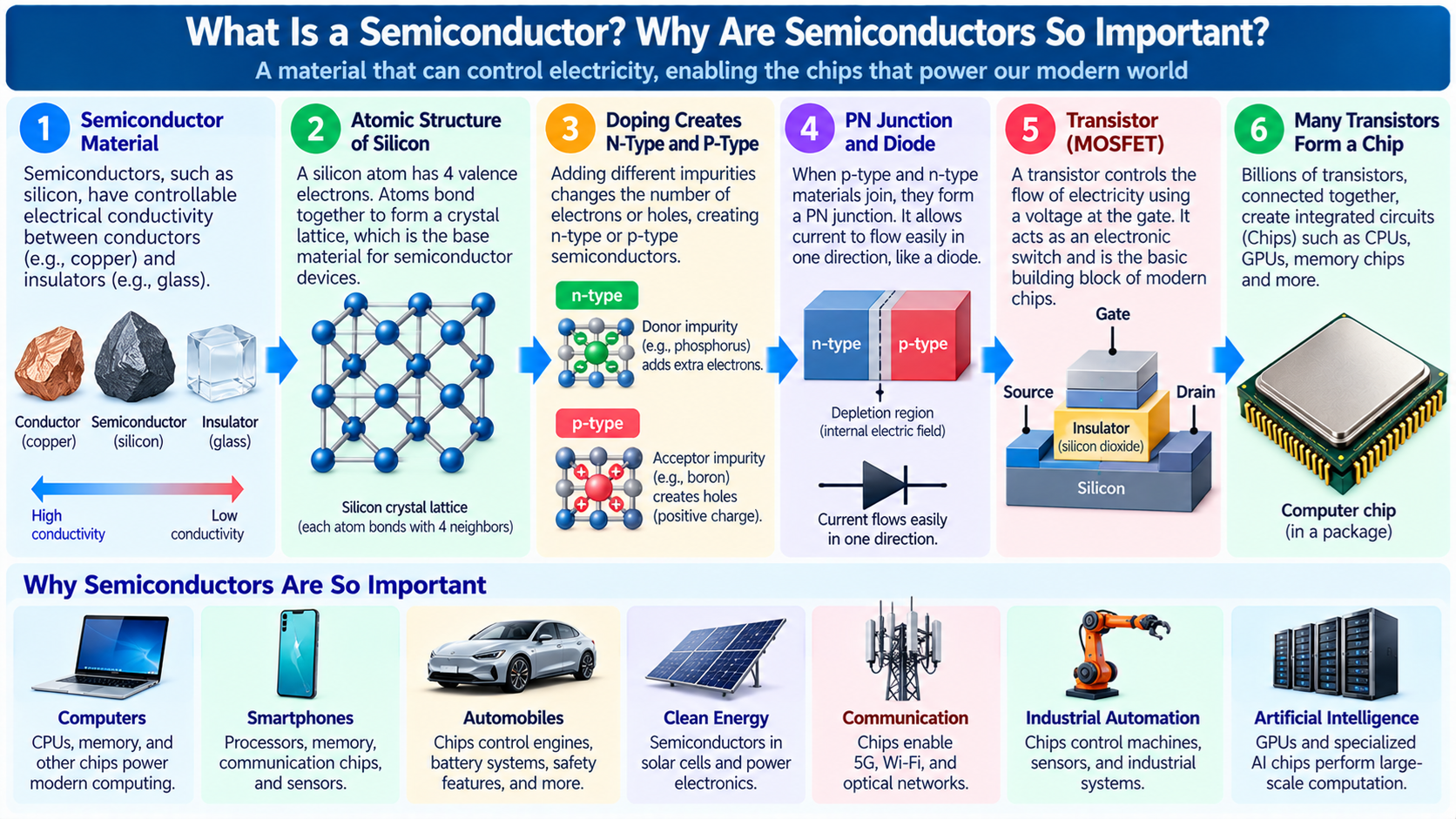
1. What Is a Semiconductor?
A semiconductor is a material whose electrical conductivity can be controlled through factors such as impurities, electric fields, temperature, and light.
Semiconductors form the foundation of modern electronic technology because they allow engineers to control electrical signals in ways that ordinary conductors and insulators cannot easily achieve.
The most widely used semiconductor material is silicon.
Silicon is used to manufacture computer processors, memory chips, microcontrollers, image sensors, power management devices, and many other electronic components.
Semiconductors are also used in solar cells, light-emitting diodes, communication equipment, industrial electronics, and electric vehicles.
A modern computer processor may contain billions of transistors fabricated from semiconductor materials.
These transistors are organized into circuits capable of performing calculations, storing information, controlling data flow, and executing software instructions.
Without semiconductor technology, modern computers, smartphones, data centers, and many automated electronic systems would be very different from those we use today.
The importance of semiconductors comes from a simple but powerful property: their electrical behavior can be engineered with remarkable precision.
By controlling how electrical charge moves through semiconductor materials, engineers can manufacture diodes, transistors, memory cells, and complex integrated circuits.
To understand why semiconductors are so important, we first need to understand how they differ from conductors and insulators.
2. What Is the Difference Between a Conductor, Insulator, and Semiconductor?
Materials behave differently when an electrical voltage is applied across them.
A conductor allows electric current to flow relatively easily. Metals such as copper, aluminum, and silver are good electrical conductors.
Copper is widely used in electrical wiring because it has low electrical resistance and can carry current efficiently.
An insulator strongly resists the movement of electric charge under ordinary operating conditions. Examples include glass, rubber, and many plastics.
Insulators are used to separate electrical conductors, protect users from electric shock, and prevent unwanted current paths.
A semiconductor occupies a different position.
In a simple introductory explanation, its electrical conductivity is often described as falling between that of a conductor and an insulator.
However, this description does not capture the most important characteristic of semiconductor materials.
The real advantage is that semiconductor conductivity can be controlled over a very wide range.
For example, engineers can add carefully selected impurities to silicon to change the number and type of available charge carriers.
They can also use electric fields to control current flowing through semiconductor devices.
This controllability makes it possible to create electronic switches, amplifiers, and other useful circuits.
A computer chip depends on semiconductor devices that can switch between different electrical states rapidly and reliably.
3. Why Is Silicon the Most Common Semiconductor Material?
Silicon is widely used in semiconductor manufacturing because it combines useful electrical characteristics with mature and highly developed manufacturing processes.
Silicon is abundant in the Earth’s crust, although producing electronic-grade silicon requires extensive purification.
Natural silicon-containing materials must be processed to obtain extremely pure silicon suitable for semiconductor fabrication.
One important advantage of silicon is its ability to form silicon dioxide, a stable insulating material that has played a major role in semiconductor device manufacturing.
Silicon dioxide can be used for electrical insulation and other purposes in integrated circuit fabrication.
Silicon also supports the controlled introduction of dopants, allowing engineers to create regions with different electrical properties.
The semiconductor industry has developed sophisticated techniques for growing silicon crystals, manufacturing wafers, creating transistors, and building complex electrical interconnections.
These processes support the large-scale production of integrated circuits.
Silicon is not necessarily the best material for every semiconductor application.
For example, gallium nitride and silicon carbide provide advantages in certain high-power or high-frequency applications.
Nevertheless, silicon remains the dominant material for general-purpose digital integrated circuits.
4. What Is a Silicon Atom?
To understand semiconductor behavior, it helps to begin with the structure of silicon atoms.
A silicon atom contains 14 protons in its nucleus and, when electrically neutral, 14 electrons surrounding the nucleus.
In a simple atomic model, silicon has four electrons in its outermost electron shell.
These are called valence electrons.
When silicon atoms form a crystal, neighboring atoms share electrons through covalent bonds.
Each silicon atom normally forms four covalent bonds with neighboring silicon atoms in the crystal structure.
This creates a repeating three-dimensional arrangement known as a crystal lattice.
The electrical properties of this structure depend on how electrons occupy allowed energy states.
At sufficiently low temperatures, an ideal pure semiconductor has very few free charge carriers available for electrical conduction.
At higher temperatures, thermal energy can excite some electrons into states where they can participate in conduction.
When an electron becomes available for conduction, it leaves behind an unoccupied state in the valence band.
This unoccupied state is called a hole.
The movement of electrons and holes is fundamental to semiconductor operation.
5. What Is an Electron and What Is a Hole?
Electrical current in semiconductor materials can be carried by electrons and holes.
An electron is a negatively charged elementary particle.
In semiconductor physics, electrons occupying available conduction-band states can move through the material and contribute to electrical current.
A hole is not a separate physical particle like an electron.
Instead, it represents an unoccupied electron state in an otherwise filled valence band.
For electrical analysis, a hole behaves like a positively charged carrier.
Imagine a row of occupied positions with one empty position.
When an electron from a neighboring position moves into the empty position, the empty position effectively shifts in the opposite direction.
Hole movement in a semiconductor can be understood in a somewhat similar way.
Both electrons and holes can contribute to electrical conduction.
In certain semiconductor regions, electrons are the majority carriers.
In other regions, holes are the majority carriers.
By controlling the concentrations of these charge carriers, engineers can construct useful electronic devices.
This is one of the most important differences between ordinary metallic conductors and semiconductor devices.
6. What Is the Energy Band Gap?
The band gap is a fundamental property of semiconductor materials.
In a crystalline solid, electrons occupy allowed ranges of energy called energy bands.
Two important bands are the valence band and the conduction band.
The valence band contains electronic states associated with bonding and other occupied states.
The conduction band contains states in which electrons can contribute to electrical conduction.
The energy difference between the valence band maximum and the conduction band minimum is called the band gap.
In a conductor, available electronic states near the Fermi level allow electrical conduction relatively easily.
In a typical semiconductor, electrons must gain sufficient energy to reach available conduction-band states.
Silicon has a band gap of approximately 1.12 electronvolts at room temperature.
This band gap is large enough to limit the number of thermally generated charge carriers, but small enough that conductivity can be controlled effectively through doping and device design.
Different semiconductor materials have different band gaps.
For example, germanium has a smaller band gap than silicon, while silicon carbide and gallium nitride have considerably larger band gaps.
Band gap differences influence device behavior, operating temperature, leakage current, optical properties, and power electronics applications.
7. What Is Semiconductor Doping?
Doping is the process of intentionally introducing selected impurity atoms into a semiconductor material to change its electrical properties.
In semiconductor manufacturing, doping allows engineers to control the concentration of electrons and holes.
For example, pure silicon has four valence electrons per atom.
If a silicon atom is replaced by a suitable impurity atom with five valence electrons, such as phosphorus, the impurity can donate an electron that contributes to conduction.
This creates an n-type semiconductor.
Alternatively, replacing silicon atoms with suitable impurities having three valence electrons, such as boron, creates acceptor states that can increase the concentration of holes.
This produces a p-type semiconductor.
Doping concentrations are carefully controlled during semiconductor manufacturing.
Different regions of a device may require different doping types and concentrations.
For example, MOSFETs use specially engineered semiconductor regions to control how electrical current moves between terminals.
Doping is one of the key technologies that makes semiconductor devices possible.
Without the ability to control material properties at microscopic scales, modern transistor and integrated circuit manufacturing would not be practical.
8. What Is an N-Type Semiconductor?
An n-type semiconductor is a semiconductor in which electrons are the majority mobile charge carriers.
It is commonly produced by introducing donor impurities into a material such as silicon.
Phosphorus, arsenic, and antimony are examples of donor dopants used in silicon.
These atoms have five valence electrons.
When incorporated into appropriate positions in the silicon crystal, they can donate electrons that become available for electrical conduction.
The donated electrons increase the conductivity of the semiconductor under suitable conditions.
However, n-type does not mean that the semiconductor is necessarily electrically negative overall.
The material is generally electrically neutral because the donated mobile electrons are balanced by positively charged ionized donor atoms.
The term n-type refers to the dominant type of mobile charge carrier.
N-type regions are used in diodes, transistors, and many other semiconductor devices.
They provide an essential part of the electrical structures used to control current flow.
9. What Is a P-Type Semiconductor?
A p-type semiconductor is a semiconductor in which holes are the majority mobile charge carriers.
It is commonly produced by adding acceptor impurities to silicon.
Boron is a widely used acceptor dopant.
A boron atom has three valence electrons, compared with silicon’s four.
When boron occupies an appropriate location in the silicon crystal, it can accept an electron from a nearby state.
This creates a hole in the valence band.
The hole can contribute to electrical conduction as neighboring electrons change their positions.
As with n-type material, a p-type semiconductor is generally electrically neutral overall.
The term p-type refers to the fact that holes are the majority mobile charge carriers.
P-type and n-type regions can be combined to construct semiconductor junctions.
These junctions are essential to diodes, bipolar transistors, solar cells, and many other electronic devices.
10. What Is a PN Junction?
A PN junction is formed when p-type and n-type semiconductor regions meet within a semiconductor structure.
The junction exhibits electrical behavior that differs from either region alone.
Initially, the carrier concentrations are different on opposite sides of the junction.
Electrons tend to diffuse from the n-type region toward the p-type region, while holes tend to diffuse in the opposite direction.
Near the junction, electrons and holes can recombine.
This process leaves behind relatively immobile ionized dopant atoms.
The resulting region contains fewer mobile carriers and is called the depletion region.
The fixed charges in this region create an internal electric field.
At equilibrium, the drift caused by this electric field balances the diffusion tendency of the carriers.
The PN junction therefore establishes an internal potential barrier that influences how current flows when an external voltage is applied.
This property allows PN junctions to perform useful functions such as rectification.
The PN junction is one of the fundamental building blocks of semiconductor electronics.
11. How Does a Semiconductor Diode Work?
A diode is an electronic device that allows current to flow much more easily in one direction than the other under ordinary operating conditions.
A simple semiconductor diode can be built using a PN junction.
When an appropriate forward voltage is applied, the potential barrier across the junction is reduced.
This allows substantial current to flow through the device.
In a typical silicon PN junction diode, noticeable forward conduction is often associated with voltages around 0.6 to 0.7 volts, although the actual voltage depends on current, temperature, and device design.
When the polarity is reversed, the depletion region generally widens and only a small reverse current flows under normal conditions.
If the reverse voltage becomes sufficiently large, breakdown may occur.
Some diodes, such as Zener diodes, are specifically designed to operate in controlled reverse breakdown regions.
Diodes are widely used in power supplies, signal processing, voltage protection, and many other circuits.
For example, rectifier diodes can convert alternating current into a unidirectional current suitable for further power supply processing.
This simple device demonstrates how semiconductor structures can control electrical current.
12. What Is a Transistor?
A transistor is a semiconductor device used to control electrical current or voltage.
Transistors can function as switches, amplifiers, and other circuit elements.
The development of the transistor was one of the most important events in the history of modern electronics.
Before transistors became widely available, many electronic systems relied on vacuum tubes.
Vacuum tubes could perform amplification and switching, but they were generally much larger and often consumed more power than semiconductor alternatives.
Transistors allowed electronic circuits to become smaller, more reliable, and more energy-efficient.
There are several types of transistors.
Two important categories are bipolar junction transistors, or BJTs, and field-effect transistors, or FETs.
Modern digital integrated circuits predominantly use MOSFET technology and its advanced variations.
A transistor does not perform complex computation by itself.
However, billions of transistors can be interconnected to create logic gates, memory cells, processors, and other digital systems.
13. How Does a MOSFET Work?
MOSFET stands for Metal-Oxide-Semiconductor Field-Effect Transistor.
A MOSFET is a voltage-controlled semiconductor device widely used in digital and analog circuits.
A conventional MOSFET has terminals called the gate, source, and drain, along with a body or substrate connection.
The gate is electrically insulated from the semiconductor channel region by a dielectric layer.
Applying a suitable voltage to the gate changes the electrical conditions in the channel region.
In a simplified enhancement-mode n-channel MOSFET, a sufficiently positive gate-to-source voltage creates a conductive channel between the source and drain.
When the gate voltage is below the appropriate threshold, the channel becomes much less conductive.
This behavior allows the MOSFET to function as an electronic switch.
Modern digital chips use enormous numbers of MOSFETs arranged into logic gates and storage circuits.
However, actual MOSFET behavior is more complex than a perfect on/off switch.
Transistors have leakage currents, capacitance, switching delays, threshold variations, and other electrical characteristics.
These properties influence chip speed, power consumption, and reliability.
14. How Do Semiconductors Create Digital Logic?
Digital computers represent information using discrete logical values, commonly called binary 0 and binary 1.
Inside semiconductor chips, these values are represented by electrical voltage ranges.
Transistors are interconnected to implement logical functions.
For example, a NOT gate produces the opposite logical value from its input.
An AND gate produces logic 1 only when all required inputs are 1.
An OR gate produces logic 1 when at least one input is 1.
An XOR gate produces logic 1 when its two inputs differ.
These simple functions can be combined into more complicated digital circuits.
For example, adders perform binary arithmetic.
Multiplexers select between data inputs.
Comparators determine relationships between binary values.
Registers store binary information.
State machines control sequences of operations.
By combining these structures, engineers create processors and other digital devices.
The most important idea is that complex computation can emerge from large arrangements of relatively simple semiconductor switching circuits.
15. What Is CMOS Technology?
CMOS stands for Complementary Metal-Oxide-Semiconductor.
It is a circuit technology that uses complementary types of MOS transistors, typically n-channel and p-channel devices.
CMOS became dominant in modern digital integrated circuits because it can provide low static power consumption in many logic applications.
Consider a simple CMOS inverter.
It uses a p-channel transistor connected toward the positive supply and an n-channel transistor connected toward the lower supply rail.
When the input is low, the p-channel transistor conducts and the n-channel transistor is largely off.
The output is driven toward the positive supply.
When the input is high, the n-channel transistor conducts and the p-channel transistor is largely off.
The output is driven toward the lower supply rail.
In a stable idealized logic state, there is no continuous direct conducting path from the positive supply to ground through both transistors.
Real circuits still consume leakage power and dynamic power during switching.
Nevertheless, CMOS provides an efficient foundation for implementing enormous numbers of logic gates.
Modern CPUs, GPUs, memory controllers, and many digital ASICs rely heavily on CMOS circuit design.
16. How Does a Semiconductor Become a Computer Chip?
A computer chip is formed by integrating many semiconductor devices into one electronic circuit.
A single transistor can control current, but a modern processor requires billions of transistors organized into useful functional blocks.
Engineers begin by designing the required logic and circuit structure.
For digital systems, hardware description languages such as Verilog and SystemVerilog are commonly used.
The design may include arithmetic units, registers, caches, control logic, and communication interfaces.
Electronic design automation tools convert the design into a representation suitable for semiconductor manufacturing.
The physical layout determines where devices and electrical connections will be placed.
Manufacturing processes then create transistors, insulating regions, contacts, and metal interconnections on a semiconductor wafer.
After fabrication and testing, individual semiconductor dies are separated from the wafer.
The dies are packaged to provide protection, electrical connections, and thermal management.
The completed packaged integrated circuits can then be installed on circuit boards or connected to other system components.
This is how semiconductor materials become functional computer chips.
17. What Is a Silicon Wafer?
A silicon wafer is a thin, circular slice of highly purified crystalline silicon.
It serves as the substrate on which many semiconductor devices and integrated circuits are manufactured.
Manufacturing typically begins with the production of high-purity silicon.
A large single-crystal silicon ingot is grown using a suitable crystal growth process.
The ingot is sliced into thin wafers, which are then processed to achieve the required surface quality.
Modern semiconductor production commonly uses wafers with diameters of 200 millimeters or 300 millimeters, depending on the fabrication technology.
A single wafer can contain many copies of the same integrated circuit design.
The number of usable dies depends on the size of the design, the wafer dimensions, manufacturing yield, and other factors.
After fabrication, the wafer is tested and cut into individual dies.
These dies are then packaged or integrated into more complex multi-die assemblies.
Wafer manufacturing is a foundational part of the semiconductor supply chain.
18. How Are Semiconductors Manufactured?
Semiconductor manufacturing involves many carefully controlled processing steps.
One of the most important techniques is photolithography.
During photolithography, a light-sensitive material called photoresist is applied to a wafer.
Selected regions are exposed using an optical patterning system.
The resulting pattern helps define where later manufacturing operations will occur.
Other important steps include deposition, etching, ion implantation, oxidation, and chemical mechanical polishing.
Deposition adds thin material layers to the wafer.
Etching removes selected material to create required structures.
Ion implantation introduces controlled quantities of dopants into selected semiconductor regions.
Oxidation can form silicon dioxide layers.
Chemical mechanical polishing helps create sufficiently flat surfaces for additional processing.
These steps are repeated many times to build transistors and interconnected circuits.
Modern semiconductor fabrication requires advanced equipment, precise measurements, and extremely clean manufacturing environments.
Even small defects can affect the functionality of a dense integrated circuit.
This is one reason semiconductor manufacturing is technologically demanding and expensive.
19. What Is a Semiconductor Fabrication Plant?
A semiconductor fabrication plant is commonly called a fab.
A fab is a specialized industrial facility used to manufacture semiconductor devices on wafers.
Modern fabs contain sophisticated equipment for lithography, deposition, etching, implantation, cleaning, inspection, and other processes.
The production environment must be carefully controlled.
Particles, chemical contamination, temperature variation, and vibration can interfere with manufacturing.
For this reason, semiconductor fabrication areas use cleanroom technology and strict contamination controls.
Some semiconductor companies both design and manufacture their own chips.
Others focus on chip design and use independent foundries for manufacturing.
A foundry is a semiconductor manufacturer that produces chips for external customers.
This separation between chip design and fabrication is an important feature of the modern semiconductor industry.
It allows companies to specialize in processor design, memory architecture, communication hardware, or other areas without necessarily owning a fabrication plant.
20. What Is the Difference Between a Foundry and a Fabless Company?
A fabless semiconductor company designs chips but generally relies on external foundries for wafer fabrication.
The company develops the architecture, logic, circuits, and physical design required for its products.
A semiconductor foundry manufactures those designs using its fabrication processes.
For example, a fabless company may design a processor or communication chip and contract a foundry to manufacture the semiconductor dies.
The completed dies may then be packaged and tested by specialized service providers.
An integrated device manufacturer, often abbreviated IDM, combines significant chip design and manufacturing activities within one company.
These business models are not always completely exclusive.
Some companies manufacture certain products internally while outsourcing others.
The foundry model has helped expand the semiconductor industry by allowing specialized design firms to develop advanced chips without bearing the full cost of operating semiconductor fabs.
However, it also creates dependence on manufacturing partners, fabrication capacity, packaging services, and global supply chains.
21. Why Are Semiconductor Manufacturing Processes So Expensive?
Advanced semiconductor fabrication requires enormous investments in equipment, buildings, infrastructure, research, and engineering.
A modern fabrication plant may contain thousands of specialized tools.
Advanced lithography systems are particularly complex because they must reproduce extremely small patterns with high precision.
Other equipment must deposit or remove thin layers while maintaining tight process control.
Manufacturers also need sophisticated inspection and measurement systems to detect defects and verify critical dimensions.
The production environment requires highly purified materials, specialized chemicals, water treatment, power distribution, and contamination control.
Developing a new manufacturing process may involve extensive research and testing.
Furthermore, not every die produced on a wafer will necessarily function correctly.
The percentage of acceptable products is called yield.
Improving yield is essential for controlling manufacturing cost.
These factors help explain why advanced semiconductor manufacturing is concentrated among companies with substantial financial and technical resources.
22. What Is Semiconductor Process Technology?
Semiconductor process technology refers to the collection of manufacturing methods and device structures used to fabricate integrated circuits.
Process generations are often identified using labels such as 28 nm, 14 nm, 7 nm, 5 nm, or 3 nm.
Historically, these labels were more closely associated with specific physical dimensions.
In modern semiconductor manufacturing, process node names are mainly technology generation labels rather than exact measurements of one transistor feature.
A newer process may provide improvements in transistor density, switching performance, or power efficiency.
However, actual results depend on the process, chip design, operating voltage, frequency, and other conditions.
A smaller process node does not guarantee that every chip manufactured using it will outperform every chip manufactured using an older process.
Many semiconductor products do not require the most advanced manufacturing technology.
For example, analog circuits, power devices, microcontrollers, and certain automotive components may use mature semiconductor processes because they provide suitable characteristics and manufacturing economics.
Advanced and mature semiconductor processes therefore remain important for different applications.
23. What Are FinFET and GAAFET Technologies?
As transistor dimensions became smaller, engineers developed new device structures to improve control over the semiconductor channel.
Traditional planar MOSFETs use a relatively flat channel configuration.
A FinFET uses a raised fin-shaped semiconductor region.
The gate surrounds multiple sides of the fin, improving electrostatic control compared with a comparable planar design.
FinFET technology has been widely used in advanced semiconductor manufacturing.
A GAAFET, or Gate-All-Around Field-Effect Transistor, uses a structure in which the gate surrounds the channel more completely.
GAAFET implementations may use nanosheets or nanowires.
These structures can improve electrostatic control and help manage leakage as transistor dimensions become smaller.
However, more advanced structures also introduce manufacturing complexity.
Different foundries may adopt different transistor architectures and process technologies.
These innovations show that semiconductor progress is not simply a matter of reducing dimensions.
It also requires changes in materials, device structures, manufacturing methods, and circuit design.
24. Why Are Semiconductors Important for CPUs and GPUs?
CPUs and GPUs are among the most recognizable products of the semiconductor industry.
A CPU executes instructions and coordinates general-purpose computation.
A GPU is designed to provide high computational throughput for graphics and suitable parallel workloads.
Both depend on semiconductor transistors and integrated circuits.
Modern processors contain large numbers of logic gates, registers, memory structures, and interconnections.
These circuits implement arithmetic operations, instruction processing, control functions, and data communication.
Advances in semiconductor technology allow engineers to integrate more computing resources and improve performance or energy efficiency under suitable conditions.
However, processor performance also depends on architecture.
A well-designed processor manufactured using an older process may outperform a less efficient design in certain workloads.
Semiconductor manufacturing provides the physical platform, while computer architecture determines how the hardware resources are organized and used.
The continued development of CPUs and GPUs therefore depends on both semiconductor technology and architectural innovation.
25. Why Are Semiconductors Important for Memory?
Modern computers require memory to store instructions, data, and intermediate results.
Semiconductor technology provides several different memory types.
SRAM, or Static Random Access Memory, is commonly used in processor caches.
A typical SRAM bit cell uses transistor circuits to maintain a stored logical state while power is supplied.
DRAM, or Dynamic Random Access Memory, commonly stores information as electrical charge in capacitive structures.
Because stored charge gradually leaks away, DRAM requires periodic refresh operations.
NAND flash memory stores information using nonvolatile semiconductor memory cells.
It is widely used in solid-state drives, smartphones, memory cards, and other storage devices.
These memory technologies involve different trade-offs among speed, density, cost, endurance, power consumption, and retention.
Semiconductor manufacturing makes it possible to integrate enormous amounts of memory into compact devices.
Without semiconductor memory, modern computing systems would not be able to provide the capacity and performance expected by today’s applications.
26. Why Are Semiconductors Important for Artificial Intelligence?
Artificial intelligence applications require substantial computing resources.
Many neural networks perform large numbers of matrix multiplications, vector operations, and other mathematical calculations.
These operations can be accelerated using specialized semiconductor hardware.
GPUs provide large-scale parallel computation and are widely used in AI training and inference.
Dedicated AI accelerators can optimize particular operations, data formats, and memory access patterns.
Modern AI chips may contain specialized matrix computation units, large on-chip buffers, high-speed interfaces, and advanced memory subsystems.
However, AI performance is not determined only by arithmetic throughput.
Memory bandwidth, memory capacity, interconnect speed, and power consumption also matter.
For example, an accelerator may have powerful arithmetic units but remain limited by the rate at which data can be supplied.
Semiconductor technology supports improvements in compute density, memory integration, and energy efficiency.
This is why semiconductor manufacturing and packaging have become important parts of modern AI infrastructure.
27. Why Are Semiconductors Important for Smartphones?
Smartphones contain many different semiconductor devices.
The application processor runs the operating system and applications.
Memory chips store active data and permanent files.
Communication chips support cellular networks, Wi-Fi, Bluetooth, and other wireless connections.
Power management integrated circuits regulate electrical power supplied to different components.
Image sensors convert incoming light into electrical signals.
Audio circuits process sound input and output.
Many smartphone processors are implemented as Systems on Chip, or SoCs.
An SoC can combine CPU cores, GPU resources, memory interfaces, multimedia engines, AI accelerators, and peripheral controllers into one integrated device.
Semiconductor integration allows smartphones to provide substantial computing capability within strict size and battery limitations.
The development of highly integrated, energy-efficient semiconductor technology is one of the main reasons modern smartphones can perform tasks that once required much larger computers.
28. Why Are Semiconductors Important for Automobiles?
Modern vehicles rely on semiconductor devices for many different functions.
Microcontrollers control electronic systems such as motor management, braking-related functions, lighting, and various sensors.
Power semiconductor devices control electrical energy flowing through motors, charging circuits, and power conversion systems.
Communication chips allow electronic control units to exchange information through automotive networks.
Advanced driver assistance systems use processors, image sensors, and other chips to interpret information from cameras, radar, and additional sensors.
Electric vehicles place especially high demands on power electronics.
For example, an electric vehicle inverter converts DC power from the battery into controlled AC power for the motor.
Semiconductor switches are essential components of this conversion process.
Automotive electronics also require high reliability and careful qualification.
Devices may need to operate across wide temperature ranges and withstand vibration, electrical disturbances, and other environmental conditions.
Semiconductors have therefore become important not only for vehicle entertainment and convenience features, but also for propulsion, control, and safety-related systems.
29. What Are Power Semiconductors?
Power semiconductors are devices designed to control or convert significant amounts of electrical power.
Examples include power MOSFETs, insulated-gate bipolar transistors, or IGBTs, and various types of power diodes.
These devices are used in power supplies, motor drives, inverters, battery charging systems, and industrial equipment.
Unlike digital logic transistors, which often operate with relatively small signals and densely integrated circuits, power semiconductor devices are optimized for handling higher currents, voltages, and thermal loads.
For example, a switching power supply uses semiconductor devices to regulate the flow of electrical energy.
The devices switch rapidly, allowing the circuit to convert electrical power efficiently.
Efficiency is important because power losses generate heat.
Reducing these losses can improve system performance and reduce cooling requirements.
Power semiconductors are especially important in electric vehicles, renewable energy systems, industrial automation, and data center power infrastructure.
30. What Are Silicon Carbide Semiconductors?
Silicon carbide, commonly abbreviated SiC, is a wide-bandgap semiconductor material.
It has physical and electrical properties that make it useful for certain high-voltage and high-temperature applications.
Compared with conventional silicon devices in suitable applications, silicon carbide power devices can support high electric fields and potentially reduce some power conversion losses.
This makes SiC attractive for electric vehicle traction inverters, charging systems, industrial drives, and other power conversion equipment.
However, silicon carbide devices are not automatically the best choice for every application.
Manufacturing cost, device availability, packaging requirements, switching behavior, and system architecture must be considered.
Silicon remains widely used in power electronics because it offers mature manufacturing processes and favorable economics for many applications.
Silicon carbide expands the range of engineering options rather than universally replacing silicon.
31. What Are Gallium Nitride Semiconductors?
Gallium nitride, or GaN, is another wide-bandgap semiconductor material.
It is used in applications that benefit from particular high-frequency, high-power-density, or optoelectronic characteristics.
GaN power transistors can support efficient high-speed switching in suitable circuit designs.
This makes them useful in certain compact power supplies, chargers, and power conversion systems.
Gallium nitride is also important in radio-frequency electronics.
Its material properties support certain high-frequency and high-power applications, including communication equipment.
In addition, GaN-based compound semiconductor structures are used in many light-emitting devices.
Blue and related LEDs have played an important role in modern lighting and display technology.
As with silicon carbide, GaN does not replace silicon in every application.
The best semiconductor material depends on electrical requirements, thermal conditions, manufacturing cost, reliability, and system design.
32. Why Are Semiconductors Important for Solar Panels?
Solar cells use semiconductor materials to convert light energy into electrical energy.
The operating principle is based on the photovoltaic effect.
When photons with sufficient energy are absorbed by a semiconductor, they can generate electron-hole pairs.
A suitable internal electric field and device structure help separate and collect these charge carriers.
This produces electrical current when the solar cell is connected to an appropriate external circuit.
Crystalline silicon is widely used in photovoltaic technology.
Other semiconductor materials are also used in specialized solar cells.
The efficiency of a solar cell depends on factors such as light absorption, recombination losses, electrical contacts, material quality, and device structure.
Solar cells demonstrate that semiconductor technology is not limited to computers.
It is also a foundation of modern renewable energy systems.
33. Why Are Semiconductors Important for LEDs?
LED stands for Light-Emitting Diode.
An LED is a semiconductor device that emits light when electrical carriers recombine under suitable conditions.
In an appropriate semiconductor junction, electrons and holes can recombine and release energy as photons.
The wavelength of the emitted light depends on the semiconductor material and device structure.
Different semiconductor materials are therefore used to produce different colors of light.
LED technology is widely used in displays, indicator lights, automotive lighting, communication systems, and general illumination.
The development of efficient blue LEDs was particularly important because it enabled practical white LED lighting through combinations of blue light and wavelength-converting materials.
LEDs are another example of semiconductor materials being used to control energy conversion rather than only electrical computation.
34. Why Are Semiconductors Important for Communication Networks?
Modern communication networks depend on semiconductor devices at nearly every stage.
Network routers and switches use integrated circuits to process packets, manage traffic, and communicate through high-speed interfaces.
Wireless equipment uses radio-frequency semiconductor devices to amplify, filter, generate, and receive signals.
Optical communication systems use semiconductor lasers, photodetectors, and electronic signal-processing circuits.
Data centers use CPUs, GPUs, memory chips, storage devices, and high-speed network interfaces.
A modern communication system may combine silicon digital processors with compound semiconductor radio-frequency or optical components.
For example, a wireless base station uses semiconductor devices for digital processing, frequency conversion, amplification, and communication control.
These functions require different circuit designs and sometimes different semiconductor materials.
The global internet therefore depends on a wide range of semiconductor technologies, not only general-purpose computer processors.
35. Why Are Semiconductors Important for Industrial Automation?
Industrial automation systems use semiconductor devices to monitor, control, and coordinate machinery.
Microcontrollers and industrial processors execute control programs.
Analog-to-digital converters turn sensor signals into digital measurements.
Power semiconductor devices control motors, actuators, and other electrical loads.
Communication interfaces connect controllers, sensors, and industrial networks.
For example, an automated production line may use semiconductor-based controllers to read sensor values, calculate control decisions, and operate motors.
Industrial systems often require predictable timing, reliability, and resistance to electrical interference.
In some applications, FPGAs are used to implement dedicated hardware processing or high-speed interfaces.
Semiconductors enable the compact, programmable, and precise control systems used throughout modern manufacturing.
36. Why Are Semiconductors Important for the Global Economy?
Semiconductors are essential components of products and infrastructure used across many industries.
Computing, telecommunications, automotive manufacturing, industrial automation, healthcare equipment, energy systems, and consumer electronics all depend on semiconductor devices.
The semiconductor supply chain includes material suppliers, equipment manufacturers, chip design companies, foundries, packaging providers, testing services, and many other organizations.
Production often involves multiple countries and specialized companies.
For example, a chip may be designed in one country, fabricated in another, packaged and tested elsewhere, and finally installed in an electronic product at a different location.
This specialization supports technological progress but also creates supply chain dependencies.
Disruptions involving manufacturing capacity, transportation, critical materials, or specialized equipment can affect many downstream industries.
The importance of semiconductors therefore extends beyond electronic engineering.
They are strategic industrial components that influence economic activity, technological capability, and infrastructure resilience.
37. What Is the Semiconductor Supply Chain?
The semiconductor supply chain includes all the activities required to turn an electronic design into a usable semiconductor product.
The process begins with research, architecture development, and circuit design.
Electronic design automation companies provide software tools used to create and verify chip designs.
Semiconductor intellectual property providers supply reusable circuit designs and technology components.
Material suppliers provide silicon wafers, chemicals, gases, and other materials.
Equipment manufacturers supply lithography, deposition, etching, inspection, and other fabrication tools.
Foundries and integrated device manufacturers fabricate semiconductor wafers.
Packaging and testing companies convert finished dies into usable products and verify their functionality.
The completed chips are then supplied to manufacturers of computers, vehicles, industrial equipment, communication systems, and other products.
Every stage has its own technical requirements.
Advanced chip production depends on the coordination of these specialized activities.
38. Why Can’t Every Country Easily Manufacture Advanced Chips?
Advanced semiconductor manufacturing requires specialized engineering knowledge, expensive equipment, reliable infrastructure, and extensive supplier networks.
A leading-edge fabrication plant cannot be created simply by constructing a building and purchasing ordinary industrial machines.
Manufacturers must develop complex process technologies, integrate specialized materials, and maintain extremely precise operating conditions.
Advanced lithography, transistor fabrication, interconnect formation, inspection, and yield optimization require years of expertise.
A successful fab also depends on trained engineers, equipment maintenance, process chemicals, high-purity materials, and other supporting industries.
Chip design requires a separate collection of capabilities, including computer architecture, digital logic, physical design, verification, and electronic design automation.
Packaging and testing introduce additional technical challenges.
Consequently, advanced semiconductor production is concentrated among a relatively limited group of manufacturers and technology suppliers.
This concentration makes semiconductor supply chains important topics in industrial policy and economic planning.
39. Are Semiconductors the Same as Computer Chips?
Semiconductors and computer chips are closely related, but they are not identical concepts.
A semiconductor is a class of material.
A computer chip is a manufactured electronic device that usually contains circuits fabricated using semiconductor technology.
For example, silicon is a semiconductor material.
A silicon wafer is a manufactured substrate used in semiconductor production.
A transistor is a semiconductor device.
An integrated circuit contains many electronic components fabricated and interconnected to perform useful functions.
A CPU is a particular kind of integrated circuit designed to execute instructions.
A packaged processor may contain one die or multiple semiconductor dies.
Therefore, the relationship can be understood as a progression from materials to devices to integrated systems.
Semiconductor materials enable transistors and other devices.
Those devices form circuits.
Circuits form chips.
Chips are connected into larger electronic systems.
This distinction is useful when studying semiconductor physics, computer architecture, FPGA design, and the chip manufacturing industry.
40. Do All Semiconductors Conduct Electricity the Same Way?
Different semiconductor materials and devices can have very different electrical behavior.
Conductivity depends on the material’s band structure, charge carrier concentrations, mobility, temperature, and other physical conditions.
For example, doping may increase the electron concentration in one semiconductor region while increasing hole concentration in another.
Applied electric fields can change the conductive state of a transistor channel.
Light can generate charge carriers in photodetectors and solar cells.
Temperature changes can influence carrier concentrations and mobility.
Different device structures use these effects for different purposes.
A digital MOSFET uses electric-field control to perform switching.
A photodiode converts absorbed light into an electrical response.
An LED converts electrical energy into emitted light.
A power transistor controls energy flow in electrical conversion equipment.
These devices may all use semiconductor materials, but their functions and operating principles are not identical.
41. Can Semiconductor Technology Continue Improving?
Semiconductor technology continues to evolve through improvements in device structures, materials, circuit architecture, manufacturing, and packaging.
For many years, transistor scaling allowed manufacturers to integrate more devices into smaller areas.
However, continued scaling faces challenges related to leakage, interconnect delay, power density, manufacturing complexity, and cost.
Engineers have developed transistor structures such as FinFETs and GAAFETs to address some of these challenges.
Advanced packaging provides another path for system improvement by connecting multiple semiconductor dies.
Chiplet architectures allow some functions to be manufactured separately and combined within a package.
New memory technologies, power semiconductor materials, and specialized accelerators also provide opportunities for progress.
For example, improving data movement and memory bandwidth can be as important as increasing the number of arithmetic units.
Future semiconductor improvements will likely involve multiple approaches rather than relying on transistor scaling alone.
The main objective remains the same: provide useful electronic functionality with suitable performance, energy efficiency, reliability, and cost.
42. What Should Beginners Learn About Semiconductors?
For beginners interested in computer chips, digital electronics, or processor design, semiconductor fundamentals provide a useful starting point.
The first topic is basic electricity.
Understanding voltage, current, resistance, and electrical power helps explain how electronic circuits operate.
The next topic is atomic structure and semiconductor materials.
Learn the meaning of valence electrons, crystal lattices, energy bands, and band gaps.
Then study electrons, holes, and semiconductor doping.
Understanding p-type and n-type materials provides the foundation for learning PN junctions.
Next, study diodes and transistors.
Learn how a MOSFET controls current and how CMOS circuits implement logic gates.
After that, explore digital logic.
Important topics include binary numbers, Boolean algebra, AND, OR, NOT, NAND, NOR, and XOR gates.
Then study combinational and sequential circuits, such as adders, multiplexers, flip-flops, registers, counters, and finite state machines.
These subjects lead naturally into CPU architecture, memory design, FPGA development, and ASIC design.
For practical experience, circuit simulators and FPGA development boards can help demonstrate how digital logic behaves.
The most effective learning path connects semiconductor physics with actual circuit behavior rather than treating the two subjects as unrelated fields.
43. Common Misunderstandings About Semiconductors
One common misunderstanding is that a semiconductor is simply a material that conducts half as well as a metal.
In reality, semiconductor conductivity can vary enormously depending on doping, temperature, electric fields, and device structure.
Another misunderstanding is that p-type material contains only positive charge while n-type material contains only negative charge.
Both materials are generally electrically neutral overall. The p-type and n-type names refer to majority mobile charge carriers.
A third misconception is that a transistor is a perfect electrical switch.
Real transistors have leakage current, switching delays, capacitance, and other nonideal properties.
Another misunderstanding is that all semiconductor devices are computer processors.
Semiconductors are used in memory, analog circuits, power electronics, sensors, LEDs, solar cells, and many other applications.
Some people also assume that smaller process node labels always indicate physically identical dimensions across manufacturers.
Modern process node names are technology labels and should not be interpreted as universal measurements of one transistor feature.
Finally, semiconductor progress does not depend only on manufacturing smaller transistors.
Architecture, materials, packaging, interconnects, memory systems, and power management are also critical.
44. From Semiconductor Materials to Modern Computing
The development of modern computing can be understood as a sequence of technological building blocks.
Semiconductor materials provide controllable electrical properties.
Doping creates regions with different charge carrier concentrations.
PN junctions and transistor structures use these properties to control electrical current.
Transistors are combined into logic gates and memory cells.
Logic gates and storage elements form arithmetic circuits, registers, state machines, and other digital structures.
These structures become processors, memory chips, controllers, and communication devices.
Multiple chips are connected through circuit boards, high-speed interfaces, and other electrical systems.
Software programs execute on processors that implement defined instruction sets.
Operating systems manage the underlying hardware and provide services for applications.
At the highest level, users interact with computers, smartphones, vehicles, and automated equipment without needing to understand the semiconductor devices inside them.
Yet the operation of these systems ultimately depends on carefully engineered materials and electronic circuits.
This connection between semiconductor physics and digital computation is one of the most important ideas in modern technology.
45. Conclusion: Why Are Semiconductors So Important?
A semiconductor is a material whose electrical behavior can be controlled through doping, electric fields, temperature, light, and other physical mechanisms.
Silicon is the most widely used semiconductor material for digital integrated circuits, but other materials such as germanium, silicon carbide, gallium nitride, and gallium arsenide are important for specialized applications.
By introducing controlled impurities, engineers create p-type and n-type semiconductor regions.
These regions can form PN junctions, while other semiconductor structures enable field-effect transistors and additional electronic devices.
Transistors are combined into logic gates, registers, memory cells, processors, and complete integrated circuits.
Semiconductor technology also supports power electronics, solar cells, LEDs, communication networks, industrial automation, automobiles, and medical equipment.
Its importance comes from the ability to manufacture extremely small, reliable, and highly integrated electronic devices that can control signals and electrical energy.
Modern computers and smartphones would not have their present capabilities without semiconductor devices.
Artificial intelligence systems depend on semiconductor processors, memory, and communication hardware.
Electric vehicles and renewable energy systems depend on semiconductor power conversion devices.
Telecommunication networks depend on semiconductor electronics and optoelectronic components.
The most important principle is simple: semiconductors make it possible to control electricity precisely, and that control allows engineers to build the electronic devices that power modern computing, communication, industry, and energy systems.
Understanding semiconductors provides the foundation for learning how transistors work, how digital circuits process binary information, how computer chips are manufactured, and why semiconductor technology has become essential to the modern world.