1. What Is a Silicon Wafer?
A silicon wafer is a thin, circular slice of highly purified crystalline silicon used as the foundation for manufacturing semiconductor devices and integrated circuits.
Silicon wafers are essential materials in the production of computer processors, memory chips, microcontrollers, communication devices, image sensors, and many other electronic components.
A silicon wafer usually has a smooth, mirror-like surface.
It may look like an ordinary reflective disc, but its material purity, crystal structure, surface quality, and dimensions are controlled with extraordinary precision.
The wafer itself is not necessarily a functioning computer chip.
A newly prepared silicon wafer is primarily a semiconductor substrate.
Transistors, insulating structures, electrical contacts, and interconnections must be manufactured on or within it before it becomes part of a functional integrated circuit.
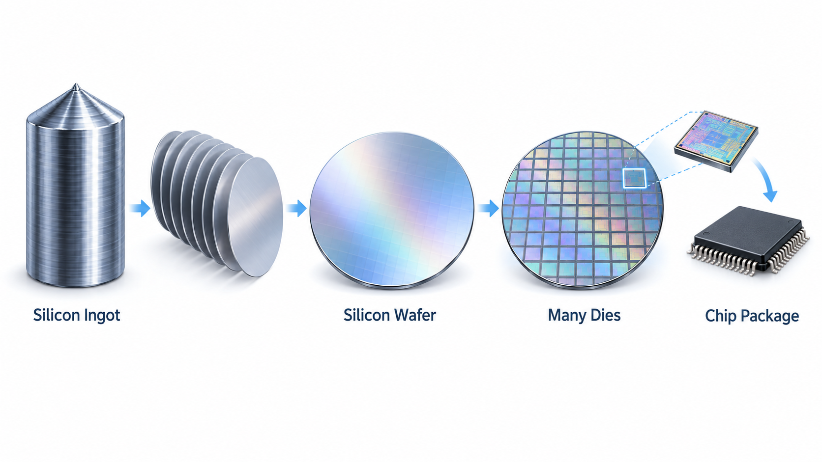
For example, a semiconductor fabrication plant may receive a 300-millimeter silicon wafer and use it to manufacture hundreds of processor dies.
Each die contains a separate copy of the processor design.
After fabrication, the wafer is electrically tested and separated into individual dies.
The usable dies are packaged to produce the chips installed in computers and other electronic systems.
Silicon wafers are therefore one of the most important starting materials in modern semiconductor manufacturing.
Understanding how wafers are made also helps explain why semiconductor production requires advanced materials science, precision machinery, cleanroom environments, and highly specialized manufacturing techniques.
2. Why Are Silicon Wafers Used to Make Computer Chips?
Modern computer chips contain enormous numbers of semiconductor devices that must be manufactured with precise electrical characteristics.
Silicon is particularly suitable for this purpose because its electrical conductivity can be controlled through doping and electric fields.
Doping introduces carefully selected impurity atoms into semiconductor material.
For example, phosphorus can be used to produce n-type silicon, while boron can be used to produce p-type silicon.
These semiconductor regions are important for constructing transistors, diodes, and other electronic devices.
Silicon also forms high-quality insulating materials, particularly silicon dioxide, which has played a major role in integrated circuit technology.
Another advantage is that silicon can be manufactured as large single crystals with highly controlled properties.
These crystals can be sliced into wafers suitable for processing in semiconductor fabrication plants.
Using wafers allows manufacturers to build many copies of an integrated circuit simultaneously.
Instead of manufacturing each processor individually, a fabrication plant processes an entire wafer containing multiple chip designs.
This wafer-level approach is essential for efficient semiconductor production.
3. What Is the Difference Between Silicon and a Silicon Wafer?
Silicon is a chemical element with the atomic number 14.
It is a semiconductor material widely used in electronic devices, solar cells, and other industrial applications.
A silicon wafer is a manufactured product made from silicon.
The wafer has been processed into a thin, circular substrate with specific requirements for diameter, thickness, crystal orientation, flatness, purity, and surface quality.
Not all silicon is suitable for manufacturing semiconductor wafers.
For example, ordinary metallurgical-grade silicon contains impurities that would be unacceptable in many advanced electronic applications.
Semiconductor-grade silicon requires much greater purity.
The material must also have suitable crystal characteristics.
Therefore, converting ordinary silicon into an electronic-grade wafer involves purification, crystal growth, cutting, polishing, cleaning, and inspection.
The difference is similar to the distinction between a raw material and a highly engineered manufacturing component.
Silicon provides the material properties, while the wafer provides a precisely prepared platform for semiconductor fabrication.
4. Why Are Silicon Wafers Round?
Silicon wafers are round mainly because of the way large single-crystal silicon ingots are commonly grown.
One widely used method is the Czochralski process.
During this process, purified silicon is melted in a controlled environment.
A small seed crystal is brought into contact with the molten silicon.
The seed is slowly pulled upward while the growing crystal and melt are controlled through suitable rotation and temperature conditions.
The silicon solidifies around the seed and forms a large cylindrical single-crystal ingot.
Because the ingot is approximately cylindrical, slicing it perpendicular to its axis produces circular wafers.
The circular shape is therefore closely related to the crystal growth process.
Round wafers also provide practical advantages for rotation-based processing and automated handling.
For example, spin coating can distribute liquid photoresist across the wafer surface.
Although the wafer is circular, most integrated circuit dies manufactured on it are rectangular.
This creates partially occupied areas around the wafer edges, where complete rectangular dies may not fit.
5. What Is a Silicon Ingot?
A silicon ingot is a large piece of crystalline silicon produced through a controlled crystal growth process.
For semiconductor wafers, manufacturers commonly grow large single-crystal ingots.
A single crystal has a continuous, ordered atomic structure across the material.
This structure is important because grain boundaries and certain other crystal imperfections can interfere with the electrical characteristics required by semiconductor devices.
The ingot is generally cylindrical and may be considerably longer than the diameter of the wafers that will eventually be produced.
After crystal growth, the ingot is inspected and processed.
Its diameter and shape may be adjusted through precision machining.
The ingot is then sliced into thin wafers.
A single ingot can provide many wafers, depending on its length, the wafer thickness, and material lost during cutting.
The silicon ingot is therefore an intermediate product between purified semiconductor silicon and finished wafers.
6. How Is Silicon Purified Before Wafer Manufacturing?
Silicon wafer manufacturing begins with high-purity silicon material.
Silicon is abundant in the Earth’s crust, usually in chemical compounds such as silicon dioxide.
Quartz is an important raw material used in silicon production.
Industrial processes first produce metallurgical-grade silicon.
However, this material is not sufficiently pure for most advanced semiconductor devices.
Further purification is necessary to remove unwanted elements.
One established production method involves converting silicon into a chemical precursor that can be purified and then used to deposit high-purity polycrystalline silicon.
The Siemens process is one widely used approach.
Electronic-grade polycrystalline silicon can have extremely low impurity concentrations.
The exact purity requirements depend on the intended semiconductor application.
Impurities such as certain metallic contaminants can alter carrier behavior, introduce defects, or reduce device reliability.
For this reason, semiconductor material purification is much more demanding than ordinary industrial silicon production.
Once the material meets the required specifications, it can be used for single-crystal growth.
7. How Is a Single-Crystal Silicon Ingot Grown?
The Czochralski process, commonly abbreviated CZ, is widely used to produce single-crystal silicon ingots for semiconductor wafers.
In a simplified description, high-purity polycrystalline silicon is placed inside a suitable crucible and heated until it melts.
A small seed crystal with a specified crystal orientation is lowered into contact with the molten silicon.
The seed is then slowly pulled upward.
Under carefully controlled conditions, additional silicon solidifies while following the crystal structure of the seed.
The growing ingot forms a continuous single crystal.
The diameter is controlled through parameters such as pulling speed and temperature.
The process may also include controlled doping to obtain the required electrical resistivity and conductivity type.
Crystal growth requires precise control because variations can introduce defects or affect material properties.
The resulting single-crystal ingot provides the starting material for wafer slicing.
8. What Is the Float-Zone Method?
The float-zone method, commonly abbreviated FZ, is another technique used to produce high-purity single-crystal silicon.
Unlike the conventional Czochralski process, float-zone crystal growth does not require the same kind of crucible containing the entire silicon melt.
Instead, a narrow molten region is created and moved through a silicon rod.
As the molten region moves, material resolidifies into the desired crystal structure.
This method can produce silicon with low oxygen content and high resistivity.
Such characteristics are valuable for certain power semiconductor devices, detectors, and specialized applications.
However, float-zone processing has different manufacturing constraints and economics from Czochralski growth.
The two methods are therefore used for different product requirements.
For mainstream high-volume digital integrated circuits, Czochralski-grown silicon is particularly important.
The existence of both methods demonstrates that wafer manufacturing is adapted to the electrical properties required by the final device.
9. How Is a Silicon Ingot Cut into Wafers?
After crystal growth, the silicon ingot must be sliced into thin discs.
This operation requires specialized precision cutting equipment.
Modern wafer manufacturing commonly uses multi-wire sawing techniques for slicing ingots.
The cutting system moves a fine wire through the silicon material while abrasive or suitable cutting mechanisms remove material.
The process creates multiple thin slices with controlled dimensions.
Each slice becomes a preliminary silicon wafer.
However, sawing introduces surface damage and dimensional variations.
The wafers may have rough surfaces, mechanical stress, and microscopic defects.
Additional processing is required before they can be used for advanced integrated circuit fabrication.
The slicing process also wastes some silicon as material is removed by the cutting operation.
This material loss is called kerf loss.
Manufacturers therefore work to balance wafer thickness, cutting accuracy, mechanical strength, and material utilization.
10. Why Must Silicon Wafers Be So Flat?
Modern semiconductor manufacturing requires highly controlled wafer surfaces.
Photolithography systems must form extremely fine patterns and align them accurately with structures created during previous operations.
An uneven wafer surface can interfere with optical focus and process consistency.
For example, if different regions of a wafer have excessive height variation, a lithography system may have difficulty maintaining the required pattern quality across the entire surface.
Surface irregularities can also affect thin-film deposition, etching, and other fabrication operations.
Manufacturers therefore control wafer flatness, thickness variation, and surface roughness.
The necessary specifications depend on the wafer and manufacturing process.
Advanced semiconductor fabrication can require particularly strict surface quality.
A wafer may appear perfectly flat to the human eye while still containing microscopic variations that are unacceptable for the intended process.
This is why wafer finishing involves specialized polishing and measurement equipment.
11. How Are Silicon Wafers Polished?
After slicing, silicon wafers undergo surface preparation to remove damage and achieve the required smoothness.
Several operations may be involved, including grinding, lapping, etching, cleaning, and polishing.
The exact sequence depends on the wafer product.
Chemical mechanical polishing, or CMP, is an important technique.
CMP uses a combination of chemical processes and mechanical action to remove material in a controlled manner.
The goal is to create a smooth and sufficiently planar wafer surface.
The process must be carefully controlled to avoid excessive material removal or damage.
A finished polished silicon wafer often has a highly reflective surface.
This mirror-like appearance is a consequence of the smooth surface finish.
However, the appearance alone does not prove that the wafer meets semiconductor manufacturing specifications.
The wafer must also satisfy requirements for flatness, roughness, particles, defects, and other material properties.
12. How Are Silicon Wafers Cleaned?
Cleaning is a critical part of silicon wafer preparation.
Even tiny particles can create serious problems during semiconductor fabrication.
For example, a particle may interfere with photolithography, contaminate a material layer, or create an unwanted electrical defect.
Wafer cleaning processes remove particles, organic residues, metallic contamination, and other unwanted materials.
Manufacturers use highly purified chemicals, ultrapure water, and specialized cleaning equipment.
Different cleaning methods target different kinds of contamination.
The cleaning process must also avoid introducing new defects or damaging the wafer surface.
After cleaning, wafers may be dried using controlled methods.
Inspection helps determine whether the wafer meets the required cleanliness standards.
Contamination control continues throughout semiconductor manufacturing.
The cleanroom environment, wafer handling equipment, processing chambers, and chemical supply systems all contribute to maintaining material quality.
13. What Is an Epitaxial Silicon Wafer?
An epitaxial silicon wafer is a wafer that has an additional crystalline semiconductor layer grown on its surface.
The process is called epitaxy.
During epitaxial growth, deposited atoms form a crystalline layer that follows the underlying substrate’s crystal orientation.
This allows engineers to create a semiconductor surface layer with controlled electrical properties.
For example, an epitaxial layer may have a different doping concentration from the underlying silicon substrate.
These characteristics can be useful for certain integrated circuits and power semiconductor devices.
Epitaxial wafers are not required for every semiconductor product.
Some manufacturing processes use polished bulk silicon wafers directly, while others require specialized substrate structures.
The choice depends on transistor design, electrical specifications, manufacturing technology, and cost.
Epitaxy is therefore an additional wafer engineering technique rather than a universal final step in every wafer production process.
14. What Is a Silicon-on-Insulator Wafer?
Silicon-on-Insulator, commonly abbreviated SOI, is a specialized wafer structure.
A typical SOI wafer contains a thin silicon device layer separated from a thicker supporting silicon substrate by an insulating layer.
The buried insulating layer is often silicon dioxide.
This structure can provide electrical isolation advantages for certain semiconductor devices.
Depending on the technology, SOI can help reduce parasitic capacitance, support particular transistor architectures, or improve selected electrical characteristics.
SOI technology has been used in digital processors, radio-frequency devices, and other specialized semiconductor products.
However, not every modern processor uses SOI wafers.
Many integrated circuits are manufactured using conventional bulk silicon substrates.
SOI wafers can be more complex and expensive to manufacture.
The decision to use SOI depends on the benefits required by the chip design and manufacturing process.
15. What Are the Common Silicon Wafer Sizes?
Silicon wafers are manufactured in several standard diameter categories.
The diameter is one of the most important dimensions because it determines the available surface area for semiconductor fabrication.
Common wafer diameters include 100 mm, 150 mm, 200 mm, and 300 mm.
These correspond approximately to the traditional 4-inch, 6-inch, 8-inch, and 12-inch wafer categories.
The inch-based labels are conventional names rather than exact metric conversions.
For example, a 300 mm wafer is commonly called a 12-inch wafer.
Different wafer sizes are used for different manufacturing technologies and applications.
Smaller wafers remain important in research, specialized devices, and certain mature processes.
200 mm wafers are widely used for various analog, power, microcontroller, and other semiconductor products.
300 mm wafers are particularly important in high-volume manufacturing of advanced logic and memory devices.
Wafer size is determined by manufacturing requirements and available equipment.
A larger wafer does not automatically mean that every chip produced on it is more advanced.
16. What Is the Difference Between 200 mm and 300 mm Wafers?
The primary difference is their diameter.
A 200 mm wafer has a diameter of 200 millimeters, while a 300 mm wafer has a diameter of 300 millimeters.
Because wafer area depends on the square of the radius, increasing the diameter substantially increases the available surface area.
The area of a circular wafer can be approximated using:
A = πr²
A 200 mm wafer has a radius of 100 mm.
Its approximate area is 31,416 square millimeters.
A 300 mm wafer has a radius of 150 mm.
Its approximate area is 70,686 square millimeters.
Therefore, a 300 mm wafer has approximately 2.25 times the surface area of a 200 mm wafer.
This can allow more dies to be manufactured during a wafer-processing cycle.
However, the actual number of usable dies depends on die size, edge losses, manufacturing defects, and yield.
Larger wafers also require compatible fabrication equipment and greater investment.
For this reason, 200 mm manufacturing remains commercially important even though 300 mm wafers dominate many advanced high-volume processes.
17. Does a Larger Wafer Produce More Chips?
A larger wafer generally provides more surface area for manufacturing integrated circuits.
If two wafers use the same chip design and manufacturing process, the larger wafer can usually accommodate more complete dies.
However, wafer area alone does not determine the final number of chips.
Suppose a processor die occupies a rectangular area on the wafer.
The dies are arranged in a grid or another suitable layout.
Because the wafer is circular, some areas near the edges cannot accommodate complete rectangular dies.
These edge losses affect the number of dies that fit.
The size of the individual die is also important.
A small microcontroller may occupy relatively little area, allowing many copies on one wafer.
A large high-performance processor may occupy much more area, reducing the number of dies per wafer.
Manufacturing defects further reduce the number of acceptable chips.
Therefore, the number of finished chips depends on wafer size, die area, layout efficiency, and manufacturing yield.
18. What Is a Semiconductor Die?
A semiconductor die is an individual piece of processed wafer containing an integrated circuit.
During wafer fabrication, many copies of a chip design are manufactured across the surface.
For example, a wafer may contain many identical processor dies.
After fabrication and testing, the wafer is cut into separate pieces.
Each piece is called a die.
The die contains the actual semiconductor devices and electrical interconnections.
A die may contain a simple circuit or billions of transistors.
However, an unpackaged die usually lacks the external connection structure required for ordinary electronic assembly.
It must be connected through suitable packaging technology.
The relationship is straightforward: the wafer is the larger substrate used during manufacturing, while the die is the individual integrated circuit obtained from that wafer.
19. How Many Chips Can Be Made from One Silicon Wafer?
There is no universal number of chips produced from one wafer.
The answer depends mainly on wafer diameter and die size.
For example, a wafer used to manufacture small control ICs may contain thousands of candidate dies.
A wafer used to manufacture large processors may contain far fewer.
The arrangement of rectangular dies on a circular wafer also affects how much area can be used.
In addition, not every manufactured die will pass testing.
Some dies may contain defects or fail electrical specifications.
The number of acceptable dies is therefore smaller than or equal to the number of candidate dies.
Chip manufacturers use specialized software and models to estimate die counts and manufacturing yield.
A rough area calculation can help beginners understand the relationship, but it should not be treated as an exact production result.
Actual manufacturing requires accounting for die dimensions, scribe lanes, edge exclusions, defects, and process-specific conditions.
20. What Happens to a Wafer Inside a Semiconductor Fab?
Once the wafer has been prepared, it is delivered to a semiconductor fabrication plant, commonly called a fab.
A fab manufactures transistors and integrated circuits through many precisely controlled processing steps.
The process may include thin-film deposition, photolithography, etching, ion implantation, annealing, cleaning, polishing, and inspection.
Photolithography defines patterns using light-sensitive materials and specialized optical equipment.
Etching removes selected material.
Ion implantation introduces dopants into semiconductor regions.
Deposition adds insulating, conductive, or semiconductor material layers.
These steps are repeated to create the required transistor and interconnect structures.
Modern integrated circuits contain multiple layers of circuitry and wiring.
The fabrication process therefore builds a complex three-dimensional structure on and within the wafer.
The wafer remains intact during most of this processing.
Individual chips are separated only after appropriate fabrication and testing operations have been completed.
21. How Are Transistors Built on a Silicon Wafer?
Transistors are manufactured by creating controlled semiconductor structures on and within the silicon wafer.
A MOSFET, for example, uses an electric field to control conduction through a semiconductor channel.
Its main device regions include the gate, source, drain, and body.
The semiconductor manufacturing process creates these structures through a combination of material deposition, doping, patterning, etching, and thermal processing.
The exact sequence depends on the transistor technology.
Traditional planar MOSFETs use relatively flat channel structures.
FinFETs use raised fin-shaped channels.
Gate-all-around transistors use structures in which the gate surrounds the channel more completely.
These device technologies require different fabrication methods.
The finished transistors are connected to form logic gates, registers, memory cells, arithmetic units, and other circuits.
A modern processor may contain billions of such transistors.
The wafer provides the physical platform on which these electronic structures are manufactured.
22. What Is Photolithography on a Silicon Wafer?
Photolithography is a technique used to transfer microscopic patterns onto a semiconductor wafer.
During the process, a light-sensitive material called photoresist is applied to the wafer.
A lithography system exposes selected regions according to the required pattern.
After development, the photoresist forms a temporary pattern.
This pattern helps guide subsequent operations such as etching or doping.
The lithography process is repeated for many different manufacturing layers.
Advanced systems must align patterns accurately with structures produced during earlier steps.
This alignment is called overlay.
Modern semiconductor manufacturing uses deep ultraviolet and, for selected advanced process layers, extreme ultraviolet lithography.
Photolithography is one of the most important technologies used to turn a prepared silicon wafer into complex integrated circuits.
However, lithography alone does not manufacture a complete transistor or processor.
It works together with deposition, etching, implantation, and other semiconductor processing techniques.
23. How Are Electrical Connections Created on a Wafer?
Transistors must be electrically connected to perform useful functions.
Modern integrated circuits contain multiple layers of conductive interconnections.
These layers connect individual transistors into logic gates and larger functional blocks.
Short connections may link nearby transistor terminals.
Longer connections may distribute power, clock signals, or data between larger regions of a chip.
The interconnect layers are separated by insulating materials.
Vertical conductive structures called vias connect different wiring levels.
The resulting network forms a complex three-dimensional arrangement above the semiconductor devices.
Manufacturing these connections requires precise patterning and material processing.
Interconnect design also affects chip performance.
Electrical resistance and capacitance can introduce signal delay and power consumption.
Therefore, semiconductor manufacturing involves creating both the transistors and the wiring that connects them.
24. What Is Wafer Testing?
After wafer fabrication, manufacturers perform electrical testing to identify semiconductor dies that meet the required specifications.
This process is commonly called wafer sort or wafer probing.
Specialized testing equipment contacts suitable electrical pads or test structures on the wafer.
The equipment applies electrical signals and measures the responses.
For example, testing may verify logic functionality, memory behavior, leakage current, or other important device characteristics.
Modern processors often contain internal structures designed to make testing easier.
Some tests help determine whether a die should be accepted, rejected, or assigned to a particular product category.
Testing before packaging can reduce manufacturing costs because defective dies may be identified before expensive assembly operations.
However, wafer testing is not always the final quality check.
Packaged chips commonly undergo additional electrical and functional testing.
25. What Is Semiconductor Yield?
Semiconductor yield describes the proportion of manufactured devices that meet specified acceptance criteria.
For example, suppose a wafer contains 100 candidate dies.
If 90 pass the relevant tests, the simplified die yield is 90 percent.
In real semiconductor manufacturing, yield analysis is more complex.
Defects can arise from particles, process variation, material contamination, patterning errors, or other causes.
The effect of a defect depends on where it occurs and the structure of the circuit.
A defect in a critical connection may cause a die to fail.
Some chip designs contain redundant structures or repair mechanisms that can improve the number of usable products.
Yield is economically important because wafer processing is expensive.
A higher percentage of functioning dies generally reduces the manufacturing cost per acceptable device.
Yield is influenced by process maturity, design characteristics, die area, defect distribution, and testing criteria.
26. What Is Wafer Dicing?
Wafer dicing is the process of separating a processed semiconductor wafer into individual dies.
During fabrication, integrated circuits are arranged across the wafer surface.
Narrow separation regions exist between the dies.
These regions are often called scribe lanes or dicing streets.
After suitable testing and preparation, specialized cutting equipment separates the wafer along these regions.
Mechanical dicing blades and laser-based techniques are among the available methods.
The process must avoid damaging the electronic circuits.
The individual dies are then handled, inspected, and prepared for packaging.
Dicing transforms a wafer containing many integrated circuits into separate semiconductor devices.
However, the dies are not necessarily finished products.
They normally require additional assembly and packaging before they can be connected to electronic systems.
27. What Happens After a Silicon Wafer Is Cut?
After dicing, the individual semiconductor dies proceed to assembly and packaging.
The exact operations depend on the product.
Some dies are attached to package substrates using flip-chip connections.
Others use wire bonding.
A package provides external electrical terminals, mechanical protection, and suitable thermal paths.
High-performance processor packages may contain a heat spreader to assist with cooling.
Advanced packages may contain multiple dies connected together.
After assembly, the packaged devices undergo electrical and functional testing.
Only products meeting the relevant specifications proceed to final distribution.
The finished chips can then be installed on circuit boards or incorporated into larger electronic systems.
This is the final transformation from a processed silicon wafer into usable electronic components.
28. What Is the Difference Between a Wafer, Die, and Chip?
These terms describe different stages or parts of semiconductor production.
A wafer is the larger circular substrate used to manufacture many semiconductor devices simultaneously.
A die is an individual piece of processed wafer containing a particular integrated circuit.
A chip is a common term that may refer to the die itself or the complete packaged electronic device.
A processor is a particular type of chip designed to execute instructions and perform computational operations.
For example, a 300 mm wafer may contain hundreds of processor dies.
After testing, the wafer is cut into individual dies.
A usable die is then assembled into a package.
The packaged processor may be installed on a motherboard or another electronic system.
Modern packages can also contain multiple dies, which is why one processor package does not always correspond to one wafer die.
Understanding these distinctions is important when discussing semiconductor manufacturing and computer hardware.
29. What Is a Silicon Wafer Notch?
Many modern silicon wafers have a small notch along the edge.
The notch provides an orientation reference for wafer handling and manufacturing equipment.
Semiconductor wafers have defined crystal orientations, and manufacturing equipment must identify the required alignment.
The notch helps automated systems determine the wafer’s orientation.
Some older or specialized wafers use flats instead of notches.
A flat is a straight section along part of the wafer edge.
These features may serve identification or orientation purposes, depending on the wafer standard and application.
The notch is not an electrical connection.
It does not indicate where the processor cores will be located.
It is primarily a mechanical and crystallographic reference used during wafer manufacturing and processing.
30. What Is Silicon Crystal Orientation?
Silicon has a crystalline structure in which atoms are arranged in an ordered three-dimensional lattice.
Different crystallographic directions and planes have different geometrical relationships.
These orientations are commonly described using crystallographic notation, such as (100), (110), and (111).
The crystal orientation can influence semiconductor processing and device characteristics.
For example, surface orientation may affect certain electrical properties, oxidation behavior, etching characteristics, and fabrication methods.
Semiconductor manufacturers therefore specify wafer crystal orientation according to the intended technology.
Not all silicon wafers use the same orientation.
The appropriate choice depends on the device design and manufacturing process.
Crystal orientation is another example of why a semiconductor wafer is a carefully engineered product rather than an ordinary slice of silicon.
31. What Is Wafer Thickness?
Wafer thickness is the distance between the two major surfaces of the silicon disc.
It is different from wafer diameter.
The diameter determines the overall circular size, while the thickness influences handling, mechanical strength, and certain processing characteristics.
A standard 300 mm silicon wafer commonly has a nominal thickness of approximately 775 micrometers, or 0.775 millimeters.
However, wafer thickness varies according to diameter, product type, and specification.
Some semiconductor manufacturing processes also involve wafer thinning.
For example, after certain fabrication steps, a wafer or die may be thinned to meet packaging or device requirements.
Thin wafers can be more difficult to handle because they are mechanically fragile.
Manufacturers must balance thickness, mechanical strength, processing compatibility, and final product requirements.
Therefore, wafer thickness is an important engineering specification rather than simply a matter of making the material as thin as possible.
32. Why Are Silicon Wafers So Expensive?
Silicon itself is abundant, but electronic-grade wafers require highly specialized manufacturing.
Producing semiconductor-grade material involves extensive purification.
Growing a large single crystal requires precise temperature control, specialized equipment, and careful material handling.
The ingot must be machined and sliced into wafers with controlled dimensions.
Each wafer then undergoes surface preparation, polishing, cleaning, and inspection.
Manufacturers must control contamination, crystal defects, flatness, and other characteristics.
Advanced wafers may also require epitaxial layers or special substrate structures.
The cost of a wafer depends on its size, material quality, specifications, production volume, and additional processing.
However, the cost of a blank silicon wafer is only one part of the total cost of a finished semiconductor chip.
Fabrication, lithography, masks, testing, packaging, yield loss, and chip development can contribute substantially more to the final product cost.
33. Why Are 300 mm Wafers Important?
The semiconductor industry moved toward larger wafers to improve manufacturing productivity.
A 300 mm wafer provides substantially more usable surface area than a 200 mm wafer.
This means more copies of a particular die design can potentially be produced during a wafer-processing cycle.
Many fabrication operations process wafers individually or in batches.
When more candidate dies fit on each wafer, the manufacturing cost per die may decrease, assuming suitable yield and production economics.
However, moving to larger wafers requires substantial equipment investment.
Handling systems, lithography equipment, deposition tools, etching equipment, and other manufacturing systems must support the larger diameter.
For many advanced logic and memory products, 300 mm production has become an important manufacturing standard.
Nevertheless, 200 mm and smaller wafers remain valuable for numerous established semiconductor technologies.
A larger wafer mainly improves manufacturing scale; it does not directly determine the computing performance of an individual chip.
34. Why Not Use 450 mm Silicon Wafers?
In principle, increasing wafer diameter beyond 300 mm could provide more surface area for manufacturing chips.
For example, a 450 mm wafer would have 2.25 times the circular area of a 300 mm wafer.
However, larger wafers introduce major technical and economic challenges.
Manufacturers would need equipment capable of handling the increased diameter and weight while maintaining precise process control.
Crystal growth, wafer flatness, vibration, thermal behavior, material handling, lithography, and other manufacturing requirements become more demanding.
A transition to a larger wafer standard also requires coordinated investment across the semiconductor equipment and materials supply chain.
The potential productivity benefits must justify the enormous cost of developing and replacing manufacturing infrastructure.
As of 2026, 300 mm remains the largest wafer diameter widely used for high-volume mainstream silicon integrated circuit manufacturing.
450 mm wafers have been studied and developed, but they have not become the standard for commercial leading-edge semiconductor production.
35. What Is a Silicon Wafer Carrier?
Silicon wafers are delicate and must be transported carefully during manufacturing.
A wafer carrier is a container or handling system designed to hold wafers while protecting them from damage and contamination.
Different carrier designs are used for different wafer sizes and processing environments.
For 300 mm semiconductor manufacturing, a common container is the Front Opening Unified Pod, or FOUP.
A FOUP holds multiple wafers in a controlled enclosure.
Automated transport systems move FOUPs between processing tools within a semiconductor fab.
The enclosure helps protect wafers from airborne particles and reduces direct human handling.
Automated wafer handling is especially important for large-scale advanced manufacturing.
It improves consistency and helps reduce contamination risks.
Wafer carriers do not perform electronic processing themselves, but they are essential supporting components of semiconductor production.
36. What Is Wafer Contamination?
Wafer contamination refers to unwanted particles, chemical residues, or impurities that may affect semiconductor manufacturing.
Contamination can originate from many sources, including processing equipment, chemicals, handling systems, and the surrounding environment.
For example, a particle on the wafer may interfere with the formation of a fine lithography pattern.
Metallic contamination can influence semiconductor electrical properties.
Organic residues may interfere with deposition or other processing steps.
Manufacturers use specialized cleaning systems, filtered environments, and process monitoring to control these risks.
Modern semiconductor fabs operate in highly controlled cleanrooms.
However, cleanliness is not limited to the room itself.
Chemical delivery systems, process chambers, wafer carriers, and internal equipment surfaces also require contamination control.
Even very small contamination levels can influence manufacturing yield.
This is one reason wafer handling and cleaning are major parts of semiconductor production.
37. How Are Silicon Wafer Defects Detected?
Wafer manufacturers use inspection and measurement techniques to evaluate material quality.
Some inspections examine the wafer surface for particles, scratches, pits, or other irregularities.
Other methods measure flatness, thickness variation, crystal defects, resistivity, and additional properties.
Optical inspection systems can detect certain surface defects.
Specialized measurement equipment evaluates physical dimensions and material characteristics.
Some techniques use electrical measurements to examine semiconductor properties.
The appropriate inspection methods depend on the wafer specification and intended application.
A defect that is acceptable for one product may be unacceptable for another.
For example, a wafer intended for a highly advanced logic process may have different requirements from a substrate used in a specialized power device.
Inspection helps manufacturers reject unsuitable material and improve production consistency.
38. What Is the Difference Between a Silicon Wafer and a Solar Wafer?
Silicon wafers are used in both integrated circuit manufacturing and photovoltaic solar cell production.
However, the two applications have different requirements.
Semiconductor wafers used for advanced integrated circuits require extremely precise surface quality, crystal characteristics, and contamination control.
Solar wafers are optimized for photovoltaic device manufacturing, cost, material utilization, and energy conversion performance.
Solar cells often use crystalline silicon wafers, but their thickness, surface treatment, and manufacturing specifications differ from those of advanced IC substrates.
A solar wafer is processed into a photovoltaic cell that converts light into electrical energy.
A semiconductor IC wafer is processed to create transistors, interconnections, and electronic circuits.
Although both may use crystalline silicon, they are not automatically interchangeable.
The manufacturing requirements are determined by the final application.
39. Are All Semiconductor Wafers Made from Silicon?
No. Silicon is the most widely used wafer material for general-purpose digital integrated circuits, but other semiconductor materials are important.
Gallium arsenide wafers are used in certain high-frequency, optoelectronic, and communication applications.
Silicon carbide wafers are important for selected high-voltage and high-power electronic devices.
Gallium nitride semiconductor layers can be grown on suitable substrates for certain power, radio-frequency, and optoelectronic devices.
Some specialized semiconductor technologies also use germanium, indium phosphide, or other materials.
Each material has particular electrical, thermal, optical, and manufacturing properties.
For example, silicon carbide can provide advantages in certain electric vehicle power conversion systems.
Gallium arsenide and related compound semiconductor technologies are useful in certain optical and radio-frequency applications.
Therefore, the term semiconductor wafer is broader than silicon wafer.
A silicon wafer is one important type of semiconductor substrate.
40. What Is the Difference Between Wafer Manufacturing and Chip Fabrication?
Wafer manufacturing and chip fabrication are related but distinct stages.
Wafer manufacturing produces the prepared semiconductor substrate.
This includes silicon purification, crystal growth, ingot shaping, slicing, surface finishing, cleaning, and inspection.
The output is a wafer ready for semiconductor device manufacturing.
Chip fabrication uses that wafer to create electronic devices and integrated circuits.
This involves processes such as lithography, deposition, etching, doping, and metal interconnection formation.
After fabrication, additional operations include electrical testing, dicing, packaging, and final testing.
Some companies specialize in producing semiconductor wafers.
Other companies operate fabs that use those wafers to manufacture integrated circuits.
Still other companies specialize in chip design, packaging, or testing.
Understanding this separation helps explain the specialized structure of the semiconductor industry.
41. How Are Silicon Wafers Used in CPU Manufacturing?
CPU manufacturing begins with an electronic processor design.
The architecture defines how instructions are executed, how data moves, and how the processor’s functional units are organized.
Engineers convert the design into a physical layout that can be manufactured using a selected semiconductor process.
The fabrication plant receives suitable silicon wafers.
Transistors and other semiconductor structures are created on the wafers through repeated processing steps.
The transistors are connected into logic gates, registers, arithmetic units, caches, and control systems.
Multiple copies of the CPU die are fabricated across each wafer.
After fabrication, the wafer is electrically tested.
Acceptable dies are separated and packaged.
Some processor products contain a single silicon die, while others combine multiple chiplets within one package.
The completed processors undergo further testing and qualification.
Thus, the silicon wafer provides the physical foundation for manufacturing the processor’s electronic circuitry.
42. How Are Silicon Wafers Used in GPU Manufacturing?
GPUs are manufactured using semiconductor processes similar in principle to those used for CPUs.
A GPU design contains many processing resources optimized for graphics and suitable parallel workloads.
The design is converted into physical patterns and manufactured on silicon wafers.
Transistors form arithmetic execution units, control logic, registers, caches, and communication circuits.
After fabrication, the GPU dies are tested and separated from the wafer.
The dies are then packaged.
High-performance GPUs and AI accelerators may require advanced packaging and high-bandwidth memory integration.
However, the exact packaging architecture depends on the product.
The silicon wafer itself does not determine whether a chip is a CPU or GPU.
That difference comes primarily from the circuit architecture implemented on the wafer.
The same general class of semiconductor substrate can support many different kinds of digital chips.
43. Why Do Wafer Manufacturers Matter to the Semiconductor Industry?
Wafer manufacturers provide the high-quality substrates required by semiconductor fabrication plants.
Without suitable wafers, even the most advanced chip design and lithography equipment cannot produce reliable integrated circuits.
Wafer quality can affect transistor characteristics, process consistency, defect levels, and manufacturing yield.
Producing large, high-quality single-crystal silicon ingots is technically demanding.
The industry requires specialized expertise in crystal growth, material purification, precision machining, polishing, cleaning, and inspection.
Wafer manufacturers must also maintain reliable supply chains and consistent product specifications.
The semiconductor industry includes specialized suppliers of silicon wafers, fabrication equipment, materials, design tools, packaging, and testing services.
Each stage contributes to the finished semiconductor product.
Wafer production is therefore a foundational industry within the larger semiconductor manufacturing ecosystem.
44. Why Are Silicon Wafers Important for Artificial Intelligence?
Artificial intelligence systems rely on advanced semiconductor processors and memory.
GPUs and specialized AI accelerators perform enormous numbers of mathematical operations.
These devices are manufactured using semiconductor technologies that depend on high-quality wafers.
Advanced processors may contain billions of transistors and complex internal connections.
Manufacturing such devices requires suitable substrates, precise fabrication, and high yields.
AI accelerators also depend on memory devices, communication chips, and power management components.
These products may use different semiconductor processes and substrate technologies.
The quality and availability of wafers therefore influence the semiconductor manufacturing capacity needed for AI infrastructure.
However, AI performance depends on much more than wafer quality.
Processor architecture, memory bandwidth, software, packaging, power consumption, and system-level design are also essential.
Silicon wafers provide the manufacturing foundation, while the completed hardware architecture determines how the computing resources are used.
45. How Can Beginners Learn About Silicon Wafers?
For beginners interested in semiconductor technology, the most useful approach is to connect wafer manufacturing with the larger chip production process.
Start by understanding what silicon is and why it behaves as a semiconductor.
Learn about electrons, holes, doping, and crystal structure.
Next, study single-crystal growth.
The Czochralski method provides a useful introduction to how semiconductor-grade silicon ingots are produced.
Then learn how ingots are sliced into wafers and why polishing, cleaning, and inspection are necessary.
After understanding wafer preparation, study semiconductor fabrication.
Important processes include photolithography, deposition, etching, ion implantation, and annealing.
Next, learn how these processes create MOSFETs and other devices.
Finally, explore how transistors become logic gates, registers, processors, and memory chips.
This sequence provides a clear connection between raw semiconductor materials and modern computing hardware.
46. Common Misunderstandings About Silicon Wafers
One common misunderstanding is that a silicon wafer is already a complete computer chip.
A newly prepared wafer normally contains no finished processor circuits. The circuits must be manufactured through subsequent fabrication steps.
Another misconception is that the wafer is simply cut from ordinary silicon.
In reality, semiconductor wafers require high-purity single-crystal material and precisely controlled surface properties.
Some people assume that all wafers are the same size.
Different wafer diameters are used for different applications and manufacturing technologies.
Another misunderstanding is that a 300 mm wafer produces chips that are inherently faster than chips made on 200 mm wafers.
Wafer diameter mainly affects manufacturing scale, while performance depends on the chip design and semiconductor process.
Some beginners also assume that every processed die will work correctly.
Manufacturing defects and variation mean that some dies may fail testing.
Finally, wafer production and chip fabrication should not be treated as the same process.
Wafer production prepares the semiconductor substrate, while fabrication creates the electronic circuitry.
47. The Complete Journey from Silicon to a Finished Chip
The journey begins with silicon-containing raw materials.
The silicon is purified to meet semiconductor manufacturing requirements.
A large single-crystal ingot is grown using an appropriate crystal growth process.
The ingot is shaped and sliced into thin circular wafers.
The wafers undergo edge finishing, cleaning, polishing, and inspection.
Some wafer products receive additional structures, such as epitaxial layers.
The prepared wafers are delivered to a semiconductor fabrication plant.
Inside the fab, repeated material processing and patterning operations create transistors and other semiconductor devices.
Multiple metal layers connect these devices into functional circuits.
The completed wafer contains many copies of the intended chip design.
Electrical testing identifies acceptable dies.
The wafer is separated into individual dies.
The usable dies are packaged and subjected to additional testing.
Finally, the packaged semiconductor devices are installed into computers, smartphones, vehicles, industrial systems, and many other electronic products.
This sequence explains how a carefully manufactured silicon substrate becomes the foundation for modern computing.
48. Conclusion: Why Are Silicon Wafers So Important?
A silicon wafer is a thin, circular substrate made from highly purified crystalline silicon.
It provides the physical foundation on which semiconductor manufacturers create transistors, memory cells, logic circuits, and complete integrated circuits.
Wafer manufacturing begins with silicon purification and crystal growth.
The resulting ingot is sliced into individual wafers, which are then polished, cleaned, inspected, and prepared for fabrication.
Different wafer sizes are used throughout the semiconductor industry.
200 mm wafers remain important in many mature and specialized processes, while 300 mm wafers are widely used for advanced high-volume logic and memory manufacturing.
A larger wafer can accommodate more candidate dies, but the number of finished chips depends on die size, edge losses, manufacturing defects, and yield.
During fabrication, each wafer undergoes many processing steps that create transistors and their electrical interconnections.
The completed wafer is tested and separated into individual dies, which are packaged to become usable semiconductor products.
The most important principle is simple: a silicon wafer is not the finished chip. It is the precisely engineered semiconductor foundation on which many chips are manufactured simultaneously.
Understanding silicon wafers provides an essential foundation for learning semiconductor materials, crystal growth, photolithography, transistor manufacturing, integrated circuits, CPUs, GPUs, memory technology, and the modern semiconductor industry.