Introduction
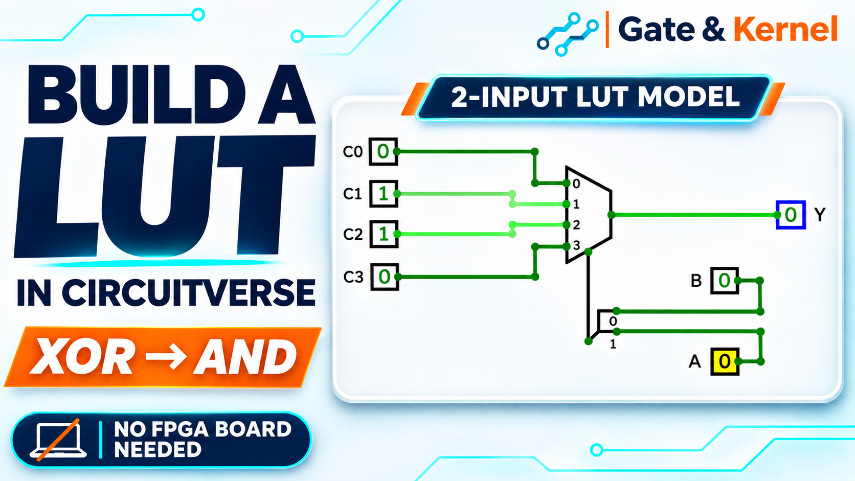
Can the same circuit perform XOR and then AND without changing its connections? In this experiment, you will make that happen by changing four configuration values.
A field-programmable gate array, or FPGA, is a chip containing digital resources whose functions and connections can be configured after manufacturing. One of those resources is a look-up table, or LUT: a structure that selects a predefined output value using its inputs.
Open CircuitVerse, a browser-based digital logic simulator, to build a small working model of this idea. You do not need an FPGA development board.
We will first verify how an input combination selects an entry. Then we will configure the model for XOR, change it to AND, and extend the idea to LUT4 and LUT6.
This is a functional model of a LUT. The switches represent stored configuration bits; we are not reproducing an FPGA’s physical memory cells or programming an actual chip.
Chapter 1: Understand the Two Different Kinds of Inputs
A bit is a binary digit whose value is 0 or 1. In this experiment, each switch supplies one bit.
Our circuit has six switches, but they have two different jobs.
A and B are the two logical inputs of the LUT. Changing them selects which stored result appears at the output.
C0, C1, C2, and C3 represent four configuration bits. Their values define the function that the LUT performs.
The output is called Y.
This distinction is essential: six visible switches do not make this a six-input LUT. We are modeling a two-input LUT with four configurable output values.
The two logical inputs have four combinations: 00, 01, 10, and 11. Throughout this article, the first digit is A and the second is B.
An address identifies a storage location. Here, the combination AB acts as the address selecting one configuration bit.
Chapter 2: What You Need
A multiplexer, usually abbreviated MUX, selects one of several data inputs and passes its value to an output. A four-to-one multiplexer selects one of four data inputs.
A bus is a group of signal bits treated as one connection. Our MUX uses a two-bit selection bus to choose among its four data inputs.
A splitter separates a bus into smaller groups of bits, or combines smaller groups into a bus. We will use it to combine A and B.
Place these components in CircuitVerse:
- Six Input elements, named A, B, C0, C1, C2, and C3.
- One Multiplexer.
- One Splitter.
- One Output element, named Y.
Choose Input, not Button, for the six switches. An Input lets you change a value and keep that state. A Button is momentary: it is high while pressed and low when released.
Set each Input and the Output to a bit width of 1. Bit width means the number of bits carried by that element.
Arrange C0 through C3 vertically on the left, the MUX in the center, and Y on the right. Put A and B near the MUX’s selection connection, leaving room for the Splitter.
Use labels and enough spacing to distinguish the configuration switches from the logical inputs.
Chapter 3: Configure the Four-to-One MUX
CircuitVerse may initially place a two-to-one multiplexer. You do not need a separate component named “4:1 MUX.”
Select the Multiplexer and set its properties:
BitWidth: 1
Control Signal Size: 2
BitWidth sets the width of each data input and the output. Control Signal Size sets the number of selection bits.
Two selection bits provide four combinations, so the MUX now has four data inputs. Their labels are normally 0, 1, 2, and 3.
Those labels are decimal port numbers. They correspond to binary selection values as follows:
| Selection value AB | Selected MUX data port | Configuration switch |
|---|---|---|
| 00 | 0 | C0 |
| 01 | 1 | C1 |
| 10 | 2 | C2 |
| 11 | 3 | C3 |
Connect each configuration switch to its matching data port. Connect the MUX’s output to Y.
The MUX also has a selection port separate from these four data ports. That is where the combined A and B signal will connect.
Chapter 4: Connect A and B Through the Splitter
Place a Splitter from the miscellaneous component category.
When asked for its total bit width, enter 2. When asked how to split that width, enter 1 1, with a space between the two digits.
This creates one two-bit connection and two single-bit branches.
A bit’s position determines its numerical weight. Bit 0 is the lower-order bit, with a weight of one. Bit 1 is the higher-order bit, with a weight of two.
Make these connections:
- B connects to the Splitter branch for bit 0.
- A connects to the Splitter branch for bit 1.
- The Splitter’s combined two-bit port connects to the MUX selection port.
Follow the bit labels rather than assuming that the upper branch is A. Component orientation can change where the branches appear.
The Splitter works in both directions, so using its branches as inputs and its combined port as an output is valid.
For example, when A is 1 and B is 0, the selection value is binary 10, or decimal 2. The MUX therefore passes C2 to Y.
Connect wires to the actual terminal dots on each component. A wire touching the edge of an Input box is not necessarily connected. In the default orientation shown by many CircuitVerse layouts, the Input’s signal terminal is on its right side.
Chapter 5: First Test Only the Address Selection
Before implementing a familiar logic function, verify that the circuit selects the correct entry.
Set the configuration switches in C0-to-C3 order to:
0, 0, 1, 0
Only C2 contains 1.
Start with A = 0 and B = 0. The address is 00, so the MUX selects C0. Y should be 0.
Change B to 1. The address becomes 01, selecting C1. Y should remain 0.
Return B to 0, then change A to 1. The address is now 10, selecting C2. Y should become 1.
Finally, change B to 1. The address becomes 11, selecting C3. Y should return to 0.
You have now observed a basic lookup: the input combination chooses one stored value.
For a complete wiring check, repeat the test with only C0 set to 1, then only C1, then only C3. Each configuration switch should appear at Y only when its matching address is selected.
This test also catches reversed A and B connections. Starting with XOR alone can hide that mistake because XOR produces the same result for 01 and 10.
Chapter 6: Configure the LUT to Perform XOR
A logic function defines an output for each input combination. Exclusive OR, abbreviated XOR, outputs 1 when two inputs differ and 0 when they match.
A truth table lists all input combinations and their corresponding outputs.
To implement XOR, set C0 through C3 to:
0, 1, 1, 0
Keep these configuration values fixed while changing A and B.
Start with both inputs at 0. The address 00 selects C0, which stores 0. Y is 0.
Change B to 1. The address 01 selects C1, which stores 1. Y becomes 1.
Return B to 0, then change A to 1. The address 10 selects C2, which also stores 1. Y is 1.
Change B to 1. The address 11 selects C3, which stores 0. Y becomes 0.
The circuit now implements XOR without using a separate XOR gate.
We have not changed the MUX into a different physical component. We have supplied the values that make its selection behavior implement the required truth table.
Chapter 7: Change the Same LUT from XOR to AND
An AND function outputs 1 only when both inputs are 1.
Leave A and B at 1. In the XOR configuration, Y is currently 0 because the selected entry, C3, contains 0.
Now change the configuration:
- Leave C0 at 0.
- Change C1 from 1 to 0.
- Change C2 from 1 to 0.
- Change C3 from 0 to 1.
The configuration is now:
0, 0, 0, 1
Because AB remains 11, the selected entry is still C3. When C3 changes to 1, Y becomes 1.
The logical inputs did not change. The circuit’s connections did not change. Its configured function changed.
Verify AND by testing the other combinations. For 00, 01, and 10, Y should be 0. For 11, Y should be 1.
In a real FPGA, configuration data is loaded through the device’s supported configuration mechanism. Manually clicking these switches is our way of demonstrating what different stored values mean.
Chapter 8: Why Two Inputs Need Four Stored Bits
Each binary input has two possible values. With two inputs, the number of combinations is two multiplied by two, which equals four.
Each combination needs one stored output value in our single-output model.
Adding another logical input doubles the number of combinations. Three inputs produce eight addresses, from 000 through 111, so a single-output three-input LUT needs eight stored bits.
In general:
A single-output LUT with K inputs requires 2 raised to the power of K stored output bits.
The number of logical inputs and the number of stored values are different quantities. The inputs select an address; the stored values define what each address returns.
Chapter 9: Extending the Idea to LUT4 and LUT6
LUT4 means a look-up table with four logical inputs. LUT6 means one with six logical inputs.
For the basic single-output model, their sizes are:
| Logical inputs | Input combinations | Stored output bits | Conceptual selector |
|---|---|---|---|
| 2 | 4 | 4 | 4:1 MUX |
| 3 | 8 | 8 | 8:1 MUX |
| 4 | 16 | 16 | 16:1 MUX |
| 6 | 64 | 64 | 64:1 MUX |
The underlying idea stays the same: a longer input address selects one value from a larger set.
For example, let a LUT4 use inputs A, B, C, and D, ordered from highest to lowest bit. The input 1010 represents decimal address 10, so it selects stored entry 10.
A LUT6 can represent any single-output Boolean function of up to six inputs by holding the appropriate output for each of its 64 combinations. It still produces one output in this basic model, not six independent outputs.
Real FPGA resources may support additional outputs or modes under architectural restrictions. Also, the conceptual selector need not be one physical, monolithic multiplexer; hardware can implement selection through smaller stages.
You do not need to place 64 switches to understand LUT6. The two-input experiment already demonstrates the essential mechanism.
Chapter 10: Optional Exercise — Build a Three-Input LUT
To extend the experiment, create a separate circuit so the original remains available.
Use an eight-to-one MUX with BitWidth set to 1 and Control Signal Size set to 3. Add three logical inputs, A, B, and C, and eight configuration switches labeled M0 through M7.
Configure a Splitter with total width 3 and split widths 1 1 1. Connect A to bit 2, B to bit 1, and C to bit 0.
Try a three-input majority function: its output is 1 whenever at least two inputs are 1.
For addresses 000 through 111, set M0 through M7 to:
0, 0, 0, 1, 0, 1, 1, 1
Test all eight combinations. For example, 001 should output 0, while 011 and 110 should output 1.
This adds one logical input and doubles the configuration storage, while preserving the same operating principle.
Chapter 11: Troubleshooting the Experiment
Y displays X
An X indicates an unknown or unresolved value. Check for disconnected terminals, an undefined selection signal, incompatible widths, or multiple sources driving the same wire.
Start with A and B. Make sure their wires attach to their actual signal terminals, not simply to the edges of their boxes.
The MUX still has only two data inputs
Set Control Signal Size to 2. Increasing BitWidth changes the width of each data path; it does not create four selectable data inputs.
A wire reports a width mismatch
The six Input elements and Y use one-bit signals. The MUX’s data width is also one bit. Only the combined selection connection carries two bits.
The configuration is correct, but the wrong entry is selected
Verify B connects to bit 0 and A to bit 1. Then run the one-entry-at-a-time test from Chapter 5 to check the MUX data-port connections.
A switch returns to 0 when released
You may have placed a Button instead of an Input. Replace it with a persistent Input element.
XOR works, but the experiment still feels confusing
Keep the configuration switches fixed and vary only A and B first. Then hold A and B fixed and change the selected configuration value. These are two different operations, and separating them makes the model easier to understand.
Conclusion
You have built a working LUT principle model, checked its address selection, configured it for XOR, and changed it to AND without changing its connections.
The distinction to remember is simple: logical inputs select an entry; configuration values define the function.
LUT4 and LUT6 extend the same mechanism to more input combinations. Understanding this small circuit gives you a practical foundation for understanding configurable logic inside an FPGA.
References
- CircuitVerse Simulator
- CircuitVerse Input Components
- CircuitVerse Multiplexer Documentation
- CircuitVerse Splitter Documentation