Introduction
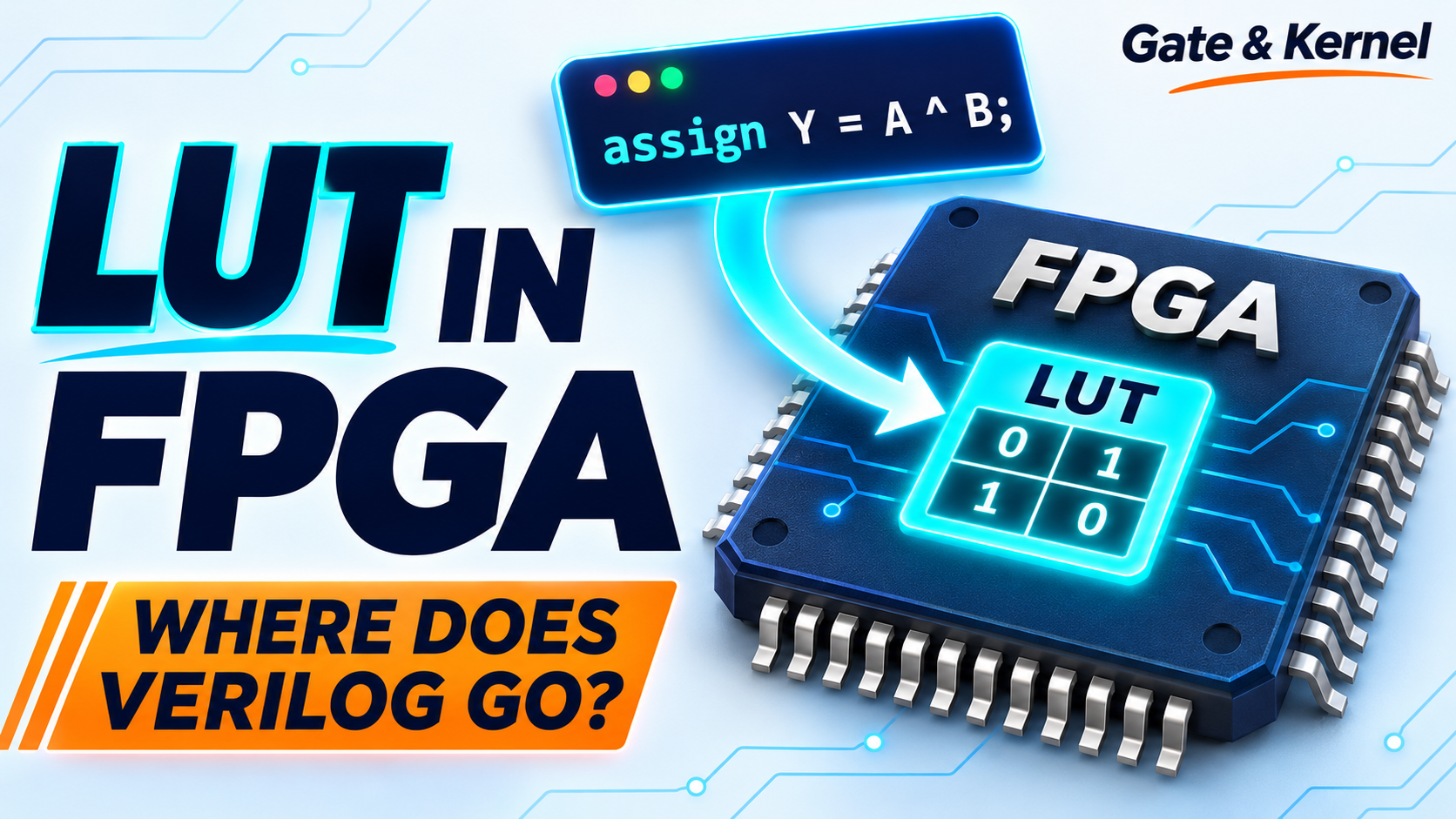
How can the same chip become a motor controller, a video processor, or a custom digital circuit without changing its physical components?
A field-programmable gate array, or FPGA, is a chip containing digital resources whose functions and connections can be configured after manufacturing. One of its most important building blocks is the look-up table, usually shortened to LUT.
A LUT implements a logic function by storing the output associated with each possible input combination. Changing these stored values changes what the circuit does.
This simple idea connects basic logic gates to real FPGA design. It also answers a practical question: when you write Verilog, where does that description go inside the chip?
Chapter 1: From Logic Gates to Truth Tables
A bit is a binary digit with a value of 0 or 1. In a digital circuit, these values represent logical states carried by electrical signals. They do not imply that every device uses exactly zero volts and one volt.
A logic gate is a circuit that produces an output according to a rule. An AND gate outputs 1 only when all its inputs are 1. An OR gate outputs 1 when at least one input is 1. A NOT gate reverses its input.
An exclusive-OR gate, or XOR gate, outputs 1 when its two inputs differ.
A truth table lists every possible input combination and its required output. For a two-input XOR function, call the inputs A and B and the output Y:
- A = 0, B = 0: Y = 0.
- A = 0, B = 1: Y = 1.
- A = 1, B = 0: Y = 1.
- A = 1, B = 1: Y = 0.
A Boolean function is a rule that maps binary inputs to a binary output. The truth table fully describes such a function.
If a circuit can select the correct output from this table, it can implement XOR without needing a separate, dedicated XOR gate for that operation.
Chapter 2: What Is a LUT?
A look-up table is a hardware structure that holds predefined output values and selects one using its inputs.
Imagine a small LUT with two inputs and one output. Two binary inputs have four possible combinations, so the LUT needs four stored output bits.
To implement XOR, store 0, 1, 1, and 0 for input combinations 00, 01, 10, and 11 respectively. When A and B are both 1, the LUT selects the entry for 11 and outputs 0.
To implement AND instead, store 0, 0, 0, and 1. The same physical LUT now performs a different function.
Two kinds of information must be distinguished. Configuration values define the function. Live input signals select which configured value appears at the output.
Changing an input does not normally rewrite the truth table. It selects a different entry in the existing table.
The FPGA design tools usually calculate these configuration values automatically. Designers describe the required behavior rather than manually filling every LUT.
Chapter 3: How Inputs Select the Output
An address is a value that identifies a storage location. In the LUT model, the input combination acts as an address selecting one stored bit.
A multiplexer, often abbreviated MUX, is a circuit that selects one of several inputs and passes it to an output. Conceptually, a two-input LUT combines four stored bits with a four-to-one multiplexer. A and B control the selection.
The selection happens through electronic circuitry. The LUT does not search the entries one by one or execute a software lookup instruction.
In many FPGAs, configuration is held in static random-access memory, or SRAM: electronic storage that retains its values while power is supplied. These devices typically reload their configuration after power is removed. Configuration technology varies across FPGA families.
A combinational circuit produces an output determined by its current inputs, after electrical delays have settled. A LUT operating as ordinary logic is combinational: it does not require a clock to select an output.
Propagation delay is the time between an input change and the resulting output change. A LUT is fast, but its delay is not zero.
Chapter 4: What Do LUT4 and LUT6 Mean?
The number in LUT4 or LUT6 describes the number of logic inputs.
A basic four-input LUT needs 16 stored output bits because four binary inputs produce 16 combinations. A six-input LUT needs 64 stored output bits because six binary inputs produce 64 combinations.
In general, a single-output LUT with K inputs needs 2 raised to the power of K stored values.
A LUT6 can implement any single-output Boolean function of up to six inputs. It does not mean six independent outputs, six instructions, or six sequential operations.
Consider the expression Y = (A AND B) OR (C AND D). Although a gate drawing shows two AND operations and one OR operation, the output depends on only four inputs. A suitable LUT can implement the complete function in one logic stage.
A logic stage is one level of combinational processing along a signal path. Combining several gate operations into one LUT can reduce the number of stages.
Larger functions may need multiple LUTs and other resources. However, input count alone does not determine the final resource count; the function’s structure and the target device also matter.
Chapter 5: Modern LUTs and FPGA Logic Blocks
Real FPGA architectures often extend the simple one-output LUT model.
A fracturable LUT is a structure that can be divided into smaller logic functions, subject to restrictions on inputs and outputs.
For example, AMD UltraScale devices support six-input LUT functions and certain combinations of two smaller functions. Two five-input functions can share a physical LUT when they use a common set of input signals. This does not provide two completely independent five-input functions with ten unrelated inputs.
An adaptive logic module, or ALM, is Altera’s configurable logic building block in families such as Agilex. It combines flexible LUT resources with storage and arithmetic circuitry. Its supported function combinations depend on the device family.
A logic block is a group of nearby configurable resources. AMD uses the term configurable logic block, or CLB, with smaller internal groupings called slices in several architectures.
Programmable routing is the network of configurable connections carrying signals between these resources.
These differences matter when reading specifications. A count of ALMs is not directly equivalent to the same count of LUTs, and an advertised logic-cell count should not automatically be treated as a physical LUT count.
Chapter 6: LUTs and Registers Do Different Jobs
A flip-flop is a circuit that stores one bit and updates it in response to a specified clock transition. A register is a storage element or group of storage elements used to hold a value.
A clock is a repeating timing signal. Its rising edge is the transition from logical 0 to logical 1.
A LUT computes a result. A register can capture that result at a clock edge and hold it for later use.
For example, a LUT may calculate whether two input signals differ. If its output connects directly to another circuit, the result changes as the inputs change. If a register captures that output, the stored result changes only on the specified clock edge, assuming its control conditions allow the update.
Sequential logic is circuitry whose behavior depends on stored state as well as current inputs. Counters and controllers need this ability to remember previous activity.
The stored bits defining a LUT’s logic function are configuration information. They are not automatically the changing state of your counter or controller.
LUTs and registers therefore complement each other: LUTs calculate relationships, while registers preserve values across time.
Chapter 7: Where Does Your Verilog Go?
Verilog is a hardware description language: a language for describing digital circuits and their behavior. SystemVerilog extends Verilog with additional design and verification features.
Consider the statement assign Y = A ^ B;, where A, B, and Y are single-bit signals. The word “assign” describes a continuous relationship, and the symbol ^ means XOR in this expression.
This statement is not an instruction that the FPGA repeatedly fetches and executes. It describes a circuit whose output is the XOR of its inputs.
Step 1: Describe and Check the Circuit
A module is a named design unit with connections called ports. The XOR statement belongs inside a module that declares A and B as inputs and Y as an output.
Simulation means testing a model of the circuit on a computer. A testbench is supporting code that supplies inputs and checks the design’s responses.
For this example, a simulation can apply all four input combinations and verify the XOR results. Simulation checks behavior, but it does not by itself establish whether the final physical circuit meets its speed requirements.
Step 2: Synthesize the Description
Synthesis translates a supported hardware description into a network of implementable circuit elements.
A netlist is a representation of those elements and their connections. Technology mapping selects resources available in the chosen FPGA to implement the required logic.
For an isolated, preserved XOR output, the tool can map the function into a LUT. In a larger design, it may combine the XOR with surrounding logic or eliminate it if its result is unused.
There is no reliable one-line-to-one-LUT relationship.
Step 3: Place and Route the Circuit
Placement chooses physical locations for circuit elements. Routing chooses the programmable connections between them.
Constraints specify design requirements, such as clock periods and assignments of external signals to chip pins. The tools use these requirements during implementation.
Timing analysis checks whether signal paths satisfy the relevant timing requirements. A circuit can be logically correct and still be too slow for the requested clock.
Step 4: Generate and Load the Configuration
A bitstream is configuration data used to program the FPGA’s resources and connections. Exact configuration-file formats depend on the device family.
The generated configuration defines LUT contents, routing choices, and other resource settings. Once loaded, the configured hardware performs the described function.
Your Verilog becomes a hardware implementation. Ordinary FPGA logic does not need a processor to interpret that source code during operation.
Chapter 8: Not Everything Becomes a LUT
FPGA tools can use several kinds of hardware resources.
A carry chain is a dedicated connection structure that efficiently transfers carry information between arithmetic stages. Addition and counting often use LUTs together with carry chains.
A digital signal processing block, or DSP block, is dedicated arithmetic hardware commonly used for operations such as multiplication and accumulation. Accumulation means adding successive results to a running total.
Block RAM is dedicated on-chip memory, separate from the LUTs used for general logic.
Depending on the description, size, settings, and target device, a multiplication may map into a DSP block, while a memory array may map into Block RAM. Smaller or differently structured operations may use other resources.
Resource inference is the tool’s recognition that a hardware description matches an available resource.
Efficient FPGA design therefore involves more than minimizing LUT count. It also involves describing circuits in ways that allow appropriate use of storage, arithmetic hardware, and routing.
Chapter 9: When LUTs Become Small Memories
Some LUT resources support additional operating modes.
Distributed RAM is small writable memory implemented using suitable resources spread through the FPGA’s logic area. RAM stands for random-access memory, meaning locations can be addressed directly.
In ordinary LUT logic mode, the stored contents define a function and normally remain unchanged during operation. In distributed RAM mode, the circuit can write application data through supported write controls.
A shift register is a sequence of storage positions that moves data along on clock events. Some FPGA LUT resources support efficient shift-register modes, useful for delays and short data buffers.
These capabilities are architecture-specific. In AMD UltraScale devices, distributed RAM is supported in memory-capable slices called SLICEMs; it is not a capability of every LUT location.
Using a resource as memory or a shift register also affects its availability for other functions. Resource sharing is subject to the device’s operating-mode restrictions.
Chapter 10: What Limits LUT Performance?
A critical path is the signal path that most tightly limits a timing requirement.
In a clocked design, a common path begins at one register, passes through routing and combinational logic, and ends at another register.
The destination register requires its input to be stable for a specified interval before capture. This is its setup time. The source register also takes time to produce its output after the clock edge.
Consequently, clock speed depends on the complete path, including routing, logic, and register timing. Counting LUTs alone cannot predict performance.
Pipelining inserts registers between processing stages so that each stage performs less work between clock edges.
Latency is the time, or number of clock cycles, from an input to its corresponding result. Throughput is the rate at which results can be produced.
A pipeline can improve achievable clock speed and throughput while adding clock cycles of latency. It must also preserve the intended alignment of data and control signals.
Chapter 11: Following a Signal Through a LUT
We can follow a complete LUT example using two input signals, A and B, and one output, Y. Imagine that the LUT is configured to perform XOR, which produces 1 when the inputs differ.
For input combinations 00, 01, 10, and 11, the stored output values are 0, 1, 1, and 0 respectively. Here, each input combination is written in the order A followed by B.
Start with A = 0 and B = 0. These inputs select the entry for 00, so Y is 0. Now change B to 1. The inputs become 01, selecting a stored value of 1. After the circuit’s propagation delay, Y becomes 1.
Next, change A to 1 while B remains 1. The inputs become 11, selecting the final entry, whose value is 0. The output therefore returns to 0 after the delay.
Throughout these changes, the stored truth table remains the same. Only the selected entry changes. The circuit is continuously responding to its inputs; it is not stepping through a list of software instructions.
Now imagine reconfiguring the same LUT to perform AND. Its stored output values become 0, 0, 0, and 1 for the same four input combinations. With A = 1 and B = 1, the output is now 1 instead of 0.
This example separates two essential ideas: input changes select results from the current function, while configuration changes define a different function. In a larger FPGA design, many such LUTs work together through programmable routing, with registers storing results wherever the circuit requires them.
Conclusion
A LUT turns a stored truth table into working combinational hardware. Its inputs select an output value, allowing the same physical structure to implement many different logic functions.
Registers add memory of previous events. Routing connects the resources. Carry chains, DSP blocks, and dedicated memories support tasks that need more than general-purpose LUT logic.
Verilog describes the required circuit. Design tools transform that description into configured resources and connections.
Understanding this process makes FPGA programming much more concrete: you are describing hardware that the tools arrange inside the chip.
Technical References
Architecture-specific details and the design-flow terminology were checked against official documentation available on November 14, 2026.
- AMD UltraScale CLB User Guide: Look-Up Table
- AMD LUT6 Primitive Reference
- Altera Agilex 7: Adaptive Logic Module
- AMD UltraScale: Distributed RAM
- AMD Vivado Design Flows Overview
- AMD Vivado Implementation Sub-Processes