Introduction
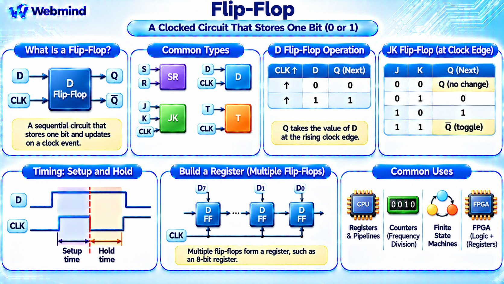
A flip-flop is a digital electronic circuit that stores one bit of binary information, either 0 or 1.
It is a fundamental building block of sequential logic and is widely used in CPUs, microcontrollers, FPGAs, ASICs, registers, counters, and digital control systems.
Unlike a combinational logic circuit, whose output depends only on its current inputs, a flip-flop can retain its state until a specified event causes it to change.
Most commonly used flip-flops are controlled by a clock signal.
They update their stored values at a particular clock edge, allowing digital circuits to perform operations in a coordinated manner.
How Does a Flip-Flop Work?
A flip-flop stores information using a circuit with two stable logical states.
Its output is commonly labeled Q, while the complementary output, when provided, is labeled Q’.
A flip-flop can retain a stored value even when its data input changes.
In a typical edge-triggered design, the stored value updates only when the appropriate clock edge occurs.
For example, a positive-edge-triggered D flip-flop copies the value of its D input to Q when the clock changes from 0 to 1.
After that clock edge, Q retains its stored value until the next triggering event or an applicable reset or set operation.
This behavior makes flip-flops essential for storing temporary information in synchronous digital systems.
Flip-Flop vs. Latch: What Is the Difference?
Flip-flops and latches are both sequential logic circuits that store binary information, but they respond differently to control signals.
Latch: A level-sensitive storage circuit. When its enable signal is active, the latch can follow changes in its data input. When the enable becomes inactive, it retains the last stored value.
Flip-Flop: Usually an edge-triggered storage circuit. It updates its output at a specified transition of the clock signal.
For example, a D latch may remain transparent while its enable input is high.
A positive-edge-triggered D flip-flop updates its stored value only at the rising edge of the clock.
This distinction is important because latches and flip-flops have different timing requirements and applications.
Main Types of Flip-Flops
Several types of flip-flops are commonly studied in digital electronics.
SR Flip-Flop
An SR flip-flop uses Set and Reset control inputs.
The Set input causes the stored output to become 1, while Reset causes it to become 0.
The exact behavior depends on whether the circuit is implemented using NAND gates, NOR gates, or a clocked structure.
In a conventional active-high SR configuration, asserting Set and Reset simultaneously is generally an invalid or restricted condition.
SR storage circuits demonstrate the basic principle of retaining a logical state.
D Flip-Flop
A D flip-flop, also called a Data flip-flop, stores the value present at its D input when the triggering clock edge occurs.
Its basic behavior is:
Q(next) = D
For a positive-edge-triggered D flip-flop, the output updates on the rising clock edge.
D flip-flops are among the most widely used storage elements in modern digital circuits.
They are commonly used in processor registers, pipelines, counters, and state machines.
JK Flip-Flop
A JK flip-flop has two control inputs, J and K.
Its conventional behavior at the active clock edge is:
J = 0, K = 0: Retain the current state.
J = 0, K = 1: Reset Q to 0.
J = 1, K = 0: Set Q to 1.
J = 1, K = 1: Toggle Q to the opposite state.
The JK flip-flop improves upon the conventional SR design by defining useful behavior when both control inputs are active.
T Flip-Flop
A T flip-flop, or Toggle flip-flop, changes its stored state when its T input is 1 at the triggering clock edge.
When T = 0, the current state is retained.
Its behavior can be expressed as:
Q(next) = Q XOR T
T flip-flops are useful for binary counters and frequency-division circuits.
For example, a T flip-flop with T permanently set to 1 toggles once per active clock edge, producing an output frequency equal to half the input clock frequency under normal operating conditions.
What Is a Clock Signal?
A clock signal is a periodic electrical signal used to coordinate operations in synchronous digital circuits.
It alternates between logical low and high states.
A rising edge occurs when the clock transitions from low to high, while a falling edge occurs when it transitions from high to low.
A positive-edge-triggered flip-flop updates on the rising edge.
A negative-edge-triggered flip-flop updates on the falling edge.
By using a shared clock, digital systems can coordinate when registers capture data and when state transitions occur.
However, real clock networks have propagation delays and timing differences known as clock skew.
These effects must be considered during hardware design.
What Are Setup Time and Hold Time?
Flip-flops require input signals to satisfy important timing constraints.
Setup Time: The minimum interval before the active clock edge during which the data input must remain stable.
Hold Time: The minimum interval after the active clock edge during which the data input must remain stable.
If these timing requirements are violated, the flip-flop may capture an incorrect value or enter a temporary condition called metastability.
Metastability occurs when the internal circuit takes an unpredictable amount of time to resolve to a stable logical state.
This is particularly important when signals cross between different clock domains.
Engineers use synchronizers, timing analysis, and appropriate clock-domain crossing techniques to reduce the risk of metastability-related failures.
What Are Reset and Set Inputs?
Many flip-flops include additional control signals.
Reset: Forces the stored output into a specified initial state, commonly 0.
Set: Forces the stored output into a specified state, commonly 1.
Reset signals may be synchronous or asynchronous.
A synchronous reset takes effect at the relevant clock edge.
An asynchronous reset can change the flip-flop state independently of the clock.
These mechanisms are important during system startup and recovery.
However, asynchronous reset deassertion requires careful timing management to avoid reliability problems.
How Are Flip-Flops Built from Transistors?
Modern flip-flops are typically implemented using CMOS transistor circuits.
A common edge-triggered D flip-flop can be built using two latch stages arranged in a master-slave configuration.
The two stages are controlled so that one captures input information while the other holds or transfers the stored value.
Other implementations use pulse-triggered structures or specialized transistor-level circuits.
The number of transistors depends on the implementation and whether the flip-flop includes reset, set, scan, or other features.
EDA tools commonly map sequential logic into optimized flip-flop cells from a semiconductor standard-cell library.
How Do Flip-Flops Build Registers?
A register is a collection of storage elements used to hold a group of binary bits.
For example, an 8-bit register can be constructed using eight D flip-flops, each storing one bit.
All eight flip-flops may share the same clock signal so that the register captures an entire binary word at the same clock edge.
A 32-bit register similarly requires storage for 32 bits.
Registers are used throughout CPUs and other digital systems to hold operands, addresses, intermediate results, and control information.
Flip-flops provide the basic storage mechanism for many register implementations.
Flip-Flops in CPUs and Pipelines
Modern CPUs use large numbers of flip-flops and other sequential storage structures.
Registers: Store processor state and temporary data.
Pipeline Registers: Hold instructions, operands, and intermediate results between processing stages.
Control State: Tracks the current state of processor control logic.
Counters: Track events, instruction-related information, and other numerical values.
Synchronizers: Help transfer certain signals safely between clock domains.
For example, a pipelined processor uses registers to separate instruction execution into multiple stages.
At each clock edge, pipeline registers capture values produced by the preceding stage.
This allows different instructions to occupy different pipeline stages simultaneously.
Flip-Flops in FPGAs
FPGAs contain configurable logic resources and large numbers of flip-flops.
These storage elements are commonly located near Look-Up Tables (LUTs) inside programmable logic blocks.
A LUT implements a combinational Boolean function, while a flip-flop stores its result when triggered by a clock.
For example, an FPGA can implement a counter by combining logic that calculates the next count value with registers that store the current count.
Many FPGA architectures also provide dedicated reset, enable, and clocking resources for sequential logic.
Understanding the relationship between LUTs and flip-flops is essential for FPGA design.
How Are Flip-Flops Described in Verilog?
Hardware Description Languages such as Verilog allow engineers to describe flip-flop behavior.
For example, a positive-edge-triggered D flip-flop can be written as:
always @(posedge clk) q <= d;
This statement describes a register that captures the D input at each rising clock edge.
The nonblocking assignment operator, represented by <=, is commonly used for sequential logic in Verilog.
Synthesis software converts the description into appropriate hardware resources.
In an FPGA, it typically maps to a dedicated register.
In an ASIC, it may map to a flip-flop standard cell.
Flip-Flops in Counters and State Machines
Flip-flops are used to construct many sequential digital circuits.
A binary counter stores its current numerical value in flip-flops and updates that value according to clock events.
For example, a four-bit counter can represent values from 0000 through 1111.
A Finite State Machine (FSM) uses flip-flops to store its current state.
Combinational logic calculates the next state based on the current state and input conditions.
At the next clock edge, the flip-flops capture the new state.
This combination of storage and logic is widely used in communication controllers, embedded systems, and processor control circuits.
Why Are Flip-Flops Important?
Flip-flops allow digital circuits to retain information and coordinate operations over time.
Without sequential storage, a circuit could perform combinational logic operations but would not have the same ability to maintain internal state.
Flip-flops make it possible to build registers, counters, synchronous pipelines, and state machines.
They also establish timing boundaries that allow engineers to analyze large digital systems systematically.
In modern semiconductor design, flip-flop timing, power consumption, and area are important factors in overall chip performance.
Conclusion
A flip-flop is a sequential digital circuit that stores one bit of binary information and typically updates its state in response to a clock edge.
Common types include SR, D, JK, and T flip-flops, with D flip-flops being especially important in modern synchronous digital systems.
Flip-flops are used to construct registers, counters, pipeline stages, and finite state machines.
They are essential components of CPUs, microcontrollers, FPGAs, ASICs, and many other digital circuits.
Understanding flip-flops provides an important foundation for studying sequential logic, clock signals, timing constraints, registers, Verilog, FPGA architecture, and digital hardware design.