Introduction
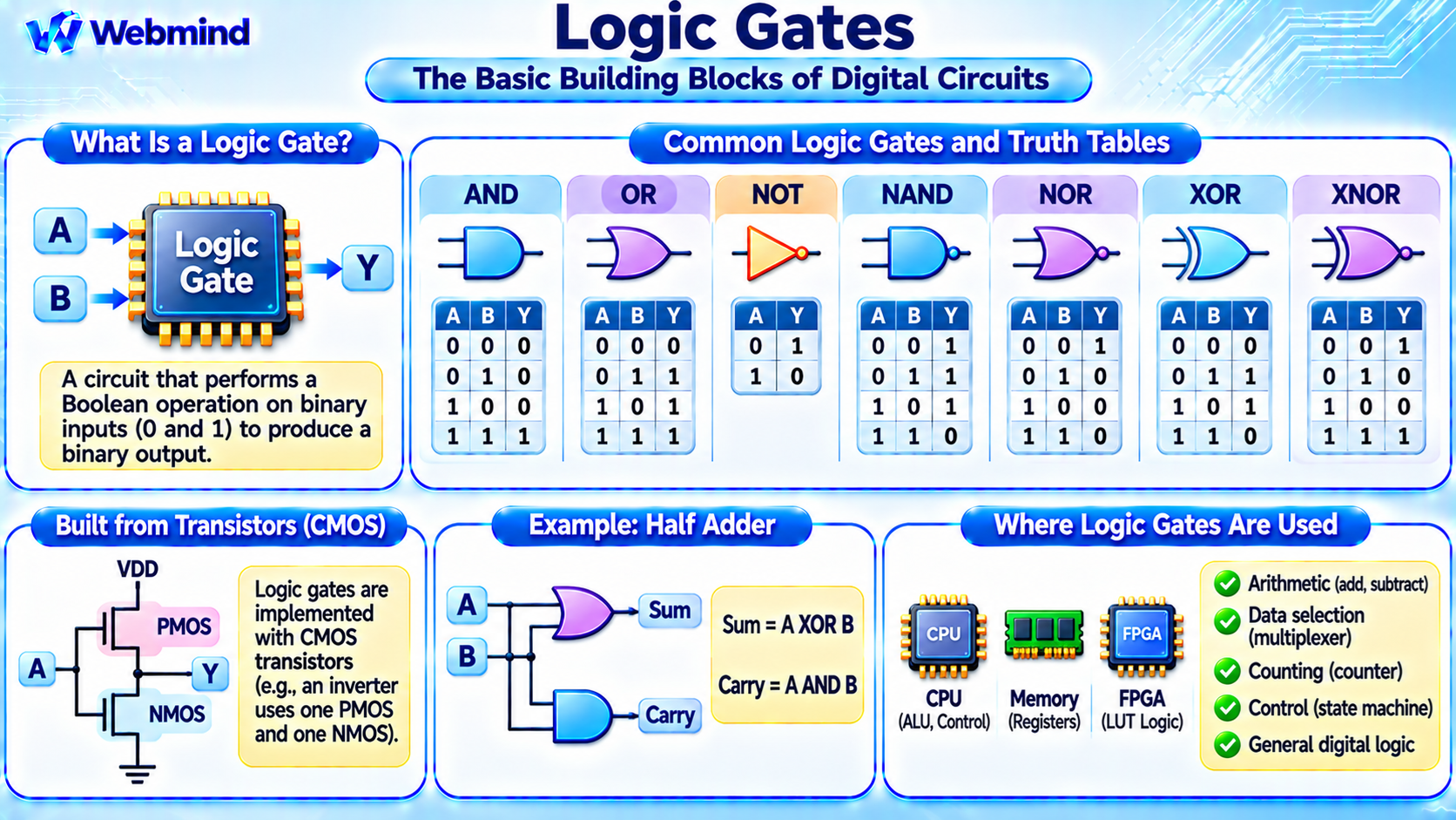
A logic gate is a fundamental building block of digital electronics that performs a Boolean operation on one or more binary inputs to produce a binary output.
Logic gates are used to build digital circuits inside CPUs, GPUs, microcontrollers, FPGAs, memory systems, and other electronic devices.
Digital logic uses two logical values: 0 and 1. In physical circuits, these values are represented by defined voltage ranges rather than exact numerical voltages.
Common logic gates include AND, OR, NOT, NAND, NOR, XOR, and XNOR.
By combining these simple operations, engineers can create complex circuits capable of arithmetic, data storage, decision-making, and processor control.
How Does a Logic Gate Work?
A logic gate receives input signals, performs a logical operation, and produces an output according to a defined rule.
For example, an AND gate with two inputs, A and B, produces an output of 1 only when both inputs are 1.
The relationship between inputs and outputs can be described using a truth table, which lists every possible input combination and its corresponding output.
Modern logic gates are typically implemented using semiconductor transistors, especially CMOS technology that combines NMOS and PMOS transistors.
Although the logical operation is mathematical, the physical circuit performs it by controlling electrical conduction and output voltage.
Main Types of Logic Gates
AND Gate
An AND gate produces 1 only when all its inputs are 1.
For a two-input AND gate:
Y = A AND B
If A = 1 and B = 1, then Y = 1. For the other three input combinations, the output is 0.
AND gates are used when multiple conditions must be satisfied simultaneously.
OR Gate
An OR gate produces 1 when at least one input is 1.
Y = A OR B
The output is 0 only when both inputs are 0.
OR gates are commonly used to combine conditions and signals in digital control circuits.
NOT Gate
A NOT gate, also called an inverter, produces the opposite logical value of its input.
Y = NOT A
If A = 0, the output is 1. If A = 1, the output is 0.
A basic CMOS inverter can be implemented using one NMOS transistor and one PMOS transistor.
NAND Gate
A NAND gate performs an AND operation followed by inversion.
Y = NOT (A AND B)
Its output is 0 only when both inputs are 1.
NAND gates are especially important because they are universal gates: any Boolean logic function can be constructed using only NAND gates.
NOR Gate
A NOR gate performs an OR operation followed by inversion.
Y = NOT (A OR B)
Its output is 1 only when both inputs are 0.
Like NAND, NOR is a universal gate and can be used to implement any Boolean logic function.
XOR Gate
An XOR gate, or Exclusive OR gate, produces 1 when its two inputs are different.
Y = A XOR B
For example, inputs 0 and 1 produce an output of 1, while inputs 1 and 1 produce an output of 0.
XOR gates are important in binary arithmetic, parity generation, and digital comparison circuits.
XNOR Gate
An XNOR gate is the inverse of an XOR gate.
It produces 1 when its two inputs have the same logical value.
XNOR gates are commonly used in equality comparisons and digital logic circuits.
What Is a Truth Table?
A truth table describes the output of a logic function for every possible combination of input values.
For a two-input AND gate, the four combinations are:
A = 0, B = 0: Output = 0
A = 0, B = 1: Output = 0
A = 1, B = 0: Output = 0
A = 1, B = 1: Output = 1
A logic circuit with n binary inputs has 2ⁿ possible input combinations.
Truth tables are useful because they provide a precise description of circuit behavior without depending on the physical implementation.
How Are Logic Gates Built from Transistors?
Modern digital integrated circuits primarily use CMOS technology to construct logic gates.
A CMOS circuit combines NMOS and PMOS transistors into complementary networks.
For example, a CMOS inverter uses one PMOS transistor connected toward the positive supply voltage and one NMOS transistor connected toward ground.
When the input is low, the PMOS conducts and pulls the output high.
When the input is high, the NMOS conducts and pulls the output low.
More complex combinations of transistors implement NAND, NOR, XOR, and other functions.
These transistor-level circuits are then combined to create larger digital systems.
How Do Logic Gates Perform Binary Addition?
Logic gates can perform arithmetic operations on binary numbers.
A half adder is a simple circuit that adds two binary digits.
It produces two outputs: Sum and Carry.
The Sum output is generated using an XOR gate:
Sum = A XOR B
The Carry output is generated using an AND gate:
Carry = A AND B
For example, when A = 1 and B = 1, the Sum output is 0 and the Carry output is 1, representing the binary result 10.
A full adder extends this idea by accepting an additional carry input.
Multiple full adders can be combined to perform arithmetic on larger binary numbers.
These circuits are fundamental components of the Arithmetic Logic Unit (ALU) inside a CPU.
Combinational vs. Sequential Logic
Digital logic circuits are commonly divided into two categories.
Combinational Logic: The output depends only on the current input values. Examples include adders, decoders, multiplexers, and basic logic gates.
Sequential Logic: The output depends on current inputs and stored internal state. Examples include counters, registers, and state machines.
Sequential circuits typically use storage elements such as flip-flops or latches.
By combining combinational and sequential logic, engineers can create processors, controllers, memory interfaces, and other complex digital systems.
Logic Gates in CPUs and Microcontrollers
Modern processors contain enormous networks of transistor-based logic circuits.
ALU: Uses logic gates to perform arithmetic, bitwise operations, and comparisons.
Control Unit: Uses logic circuits to decode instructions and generate control signals.
Registers: Use storage circuits to hold temporary data and processor state.
Multiplexers: Select between different data sources.
Decoders: Translate binary input combinations into control signals.
Counters: Track events, addresses, or timing-related values.
These circuits operate together to execute machine instructions and control processor activity.
How Are Logic Gates Used in FPGAs?
An FPGA, or Field-Programmable Gate Array, is a programmable semiconductor device that can implement many different digital logic circuits.
Unlike fixed-function ASIC logic, FPGA logic can be configured after manufacturing.
Modern FPGAs commonly use Look-Up Tables (LUTs) to implement combinational logic functions.
A LUT stores the output values of a truth table and selects the appropriate output based on its binary inputs.
For example, a two-input AND gate has four possible input combinations.
A LUT can implement this AND function by storing the output pattern 0, 0, 0, 1 for the corresponding input combinations.
The same LUT can be reconfigured to implement OR, XOR, NAND, or another compatible logic function.
FPGA registers and programmable routing resources allow these functions to form larger sequential circuits and complete digital systems.
This is an important connection between Boolean logic, truth tables, and FPGA hardware architecture.
What Is Propagation Delay?
Real logic gates do not change their outputs instantaneously.
Propagation delay is the time required for a change at a gate input to produce the corresponding change at its output.
This delay depends on factors such as transistor characteristics, supply voltage, output load, and temperature.
When several gates are connected in a chain, their delays contribute to the total delay of the circuit.
For example, a long combinational path between two registers may limit the maximum clock frequency of a digital system.
Engineers use timing analysis to ensure that digital circuits operate reliably within their required timing constraints.
Why Are Logic Gates Important?
Logic gates provide the connection between Boolean mathematics and physical electronic circuits.
They allow engineers to implement decisions, arithmetic operations, comparisons, and control functions using binary signals.
Simple gates can be combined to create adders, multiplexers, counters, registers, and state machines.
These components form the foundation of CPUs, GPUs, FPGAs, ASICs, microcontrollers, and other digital systems.
Understanding logic gates is therefore essential for studying digital electronics, computer architecture, and hardware design.
Conclusion
A logic gate is an electronic circuit that performs a Boolean operation on binary inputs to produce a binary output.
AND, OR, NOT, NAND, NOR, XOR, and XNOR are the main types of logic gates used in digital systems.
Modern logic gates are typically implemented using CMOS transistors and combined into larger combinational and sequential circuits.
In CPUs, they perform arithmetic and control operations. In FPGAs, configurable LUTs implement the same Boolean functions using stored truth-table values.
Understanding logic gates provides an essential foundation for learning Boolean algebra, binary arithmetic, CPU architecture, Verilog, FPGA development, and digital integrated circuit design.