Introduction
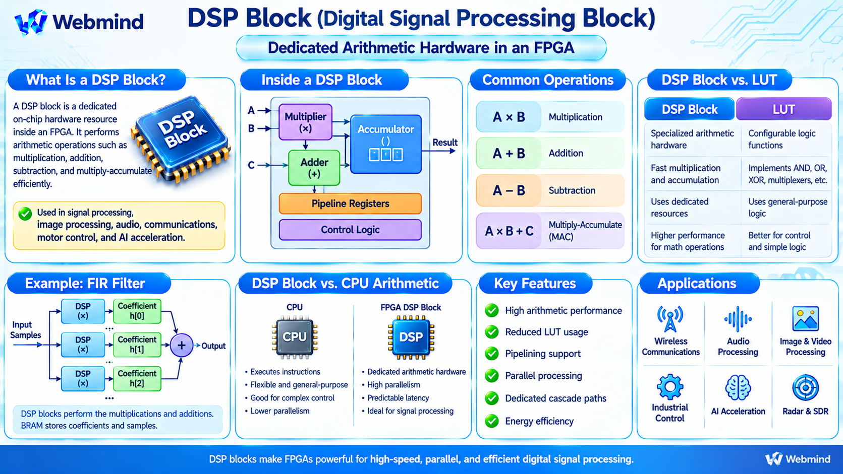
A DSP Block, or Digital Signal Processing Block, is a dedicated arithmetic hardware resource inside a Field-Programmable Gate Array (FPGA).
It is designed to perform mathematical operations such as multiplication, addition, subtraction, and multiply-accumulate calculations efficiently.
Unlike general-purpose FPGA logic built from Look-Up Tables (LUTs), DSP blocks contain specialized arithmetic circuits manufactured directly into the chip.
DSP blocks are widely used in digital signal processing, image processing, audio systems, wireless communications, motor control, and artificial intelligence acceleration.
They allow FPGA designers to perform complex mathematical operations at high speeds while reducing the amount of programmable logic required.
How Does a DSP Block Work?
A DSP block receives numerical inputs, performs arithmetic operations, and produces a result.
For example, a basic DSP block may multiply two binary numbers, A and B, and generate their product.
More advanced configurations can combine multiplication with addition or accumulation.
A common operation is multiply-accumulate, usually abbreviated as MAC.
The mathematical expression is:
P = A × B + C
Here, A and B are multiplied, and the result is added to C.
In an accumulation configuration, C may represent a previously stored result, allowing repeated multiplication and accumulation over successive clock cycles.
Many DSP blocks also contain pipeline registers that help the arithmetic circuits operate at high clock frequencies.
The exact capabilities depend on the FPGA architecture.
Main Components of a DSP Block
A modern FPGA DSP block may contain several important hardware components.
Multiplier: Performs binary multiplication on input operands.
Adder/Subtractor: Adds or subtracts numerical values.
Accumulator: Stores and updates intermediate arithmetic results.
Pipeline Registers: Hold data between arithmetic stages to improve timing performance.
Control Logic: Selects arithmetic operations and controls internal data paths.
Cascade Connections: Allow neighboring DSP blocks to exchange intermediate results efficiently.
Some DSP architectures also support pre-adders, comparison functions, pattern detection, and specialized numerical operations.
These features vary between FPGA manufacturers and product families.
What Is Multiply-Accumulate (MAC)?
Multiply-accumulate is one of the most important operations performed by DSP hardware.
A MAC operation multiplies two numbers and adds the product to an accumulated value.
For example:
Accumulator = Accumulator + A × B
Suppose the accumulator initially contains zero.
If A = 3 and B = 4, the first operation produces 12.
If the next inputs are A = 2 and B = 5, the accumulated result becomes:
12 + 2 × 5 = 22
MAC operations are fundamental to digital filters, matrix multiplication, image processing, and neural network calculations.
Because these applications repeatedly perform multiplication and addition, dedicated MAC hardware can provide significant performance advantages.
DSP Blocks vs. LUTs
DSP blocks and LUTs are both important FPGA resources, but they serve different purposes.
LUT: Implements configurable Boolean logic functions such as AND, OR, XOR, multiplexers, and control equations.
DSP Block: Implements specialized arithmetic operations using dedicated hardware circuits.
For example, a binary multiplier can be constructed using LUTs and registers.
However, a dedicated DSP block can often perform the same operation more efficiently in terms of logic resource usage, operating frequency, and power consumption.
Using DSP blocks also preserves LUT resources for other parts of the FPGA design.
Nevertheless, simple arithmetic operations may still be implemented efficiently using general-purpose logic and dedicated carry chains.
DSP Blocks vs. CPU Arithmetic Units
Both CPUs and FPGA DSP blocks perform arithmetic operations, but their architectures differ.
A CPU executes instructions using arithmetic units controlled by software and processor hardware.
An FPGA can configure multiple DSP blocks into dedicated arithmetic pipelines.
For example, a CPU may execute a sequence of multiplication and addition instructions to process a stream of sensor samples.
An FPGA can construct a pipeline containing multiple DSP blocks that operate on different samples simultaneously.
This can provide high throughput and predictable processing latency.
However, FPGA DSP blocks are not automatically faster than modern CPU vector units or GPU arithmetic hardware.
Actual performance depends on numerical precision, memory bandwidth, algorithm structure, clock frequency, and system architecture.
What Is Pipelining in a DSP Block?
Pipelining divides an arithmetic operation into multiple stages separated by registers.
For example, a multiplication operation may use input registers, internal pipeline registers, and an output register.
Each stage processes part of the operation while other stages work on different input data.
After the pipeline is filled, a DSP block may produce one result per clock cycle, depending on its configuration.
Pipelining can improve the maximum operating clock frequency.
However, it also increases latency because data must pass through multiple registered stages.
FPGA designers balance throughput, latency, and register configuration according to application requirements.
What Are DSP Cascade Connections?
Some FPGA architectures provide dedicated connections between neighboring DSP blocks.
These are commonly called cascade paths.
A cascade connection allows the output or intermediate result of one DSP block to feed another DSP block without relying entirely on general-purpose FPGA routing.
For example, several DSP blocks may be connected to implement a long arithmetic accumulation chain.
Dedicated cascade routing can reduce delays and conserve programmable interconnection resources.
These connections are especially useful in digital filters, large arithmetic pipelines, and signal-processing applications.
Their availability and configuration depend on the target FPGA family.
DSP Blocks in Digital Filters
Digital filters are among the most common applications of FPGA DSP blocks.
A Finite Impulse Response (FIR) filter processes input samples using a set of coefficients.
A simplified FIR calculation is:
y[n] = Σ h[k] × x[n − k]
Here, x represents input samples, h represents filter coefficients, and y represents the filtered output.
Each coefficient is multiplied by a corresponding sample, and the products are added together.
DSP blocks perform the multiplication and accumulation operations.
Block RAM or distributed memory may store coefficients and sample data, while registers provide pipelining.
This combination allows FPGAs to process high-speed signal streams efficiently.
DSP Blocks in Image and Video Processing
Image-processing algorithms frequently require arithmetic operations on pixel values.
For example, an image filter may multiply neighboring pixel values by predefined coefficients and sum the results.
DSP blocks can accelerate these calculations.
Applications include image sharpening, blurring, edge detection, color conversion, and video scaling.
A typical FPGA video-processing pipeline may use Block RAM for line buffers, DSP blocks for arithmetic calculations, and LUTs for control logic.
Because these operations can be pipelined, an FPGA may process multiple stages of an image-processing algorithm concurrently.
DSP Blocks in Artificial Intelligence
Artificial intelligence workloads often involve large numbers of multiplication and accumulation operations.
Neural networks perform calculations involving weights, activations, and intermediate numerical results.
For example, a neural network layer may calculate a weighted sum:
Y = W1 × X1 + W2 × X2 + W3 × X3
DSP blocks can implement these multiplications and additions.
Multiple DSP blocks can operate in parallel to accelerate neural network inference.
Some newer FPGA families also provide specialized AI-oriented arithmetic resources beyond conventional DSP blocks.
However, AI acceleration performance depends on memory bandwidth, data representation, parallelism, and the architecture of the complete accelerator.
DSP blocks are therefore one important part of FPGA-based AI computing.
Fixed-Point vs. Floating-Point DSP
Digital arithmetic can use different numerical representations.
Fixed-Point Arithmetic: Represents numbers using a fixed scaling factor or binary-point position.
Fixed-point arithmetic is common in embedded signal processing because it can be implemented efficiently in hardware.
Floating-Point Arithmetic: Represents numbers using a significand and exponent, supporting a much wider range of magnitudes.
Floating-point processing is useful in scientific computing and applications requiring wide dynamic range.
Many traditional FPGA DSP blocks are optimized for integer or fixed-point multiplication and accumulation.
Floating-point operations may require additional FPGA logic, multiple DSP blocks, or dedicated floating-point hardware in supported architectures.
The appropriate representation depends on numerical accuracy, resource usage, and performance requirements.
What Are DSP Block Widths?
DSP blocks support specific operand and result widths determined by their hardware architecture.
For example, a DSP multiplier might support an 18-bit by 18-bit multiplication, a 27-bit by 18-bit multiplication, or another configuration.
The product of two unsigned n-bit numbers may require up to 2n bits to represent the full result.
For example, multiplying two unsigned 8-bit numbers can require a 16-bit result.
Larger arithmetic operations may need multiple DSP blocks or additional logic.
Some DSP architectures also support SIMD-style arithmetic, allowing several narrower operations to share one hardware block.
FPGA designers must understand these width constraints to avoid overflow, truncation, or unexpected numerical behavior.
How Are DSP Blocks Used in Verilog?
FPGA developers typically describe arithmetic operations using Verilog or SystemVerilog.
For example, a multiplication may be described as:
assign p = a * b;
A multiply-accumulate operation may be described as:
p <= p + a * b;
The second expression would normally appear inside a clocked process with appropriate signal declarations and reset behavior.
During synthesis, an EDA tool analyzes the arithmetic expression and may map it to dedicated DSP resources.
DSP inference depends on operand widths, signedness, register placement, target architecture, and synthesis settings.
For more precise control, designers may instantiate vendor-specific DSP primitives or IP blocks.
Understanding numerical widths and pipeline timing is essential for obtaining correct results.
DSP Blocks in AMD and Intel FPGAs
Different FPGA manufacturers provide different DSP architectures.
AMD DSP Resources: AMD FPGA families include dedicated DSP slices that support multiplication, accumulation, arithmetic operations, and configurable internal registers.
Intel DSP Resources: Intel FPGA families provide dedicated DSP blocks with multiplication, accumulation, and other arithmetic capabilities.
The supported operand widths, pipeline structures, cascade connections, and numerical features vary by device generation.
Some advanced FPGA and adaptive computing devices also integrate specialized processing resources alongside conventional DSP blocks.
Therefore, the capabilities of a DSP block should always be checked against the documentation for the selected device.
How Is DSP Utilization Measured?
FPGA implementation tools report how many DSP resources are used by a design.
For example, suppose an FPGA contains 1,000 available DSP blocks and a design uses 250.
The simplified utilization is:
250 ÷ 1,000 × 100% = 25%
Actual resource reports may use DSP slices, multiplier units, or other architecture-specific resource categories.
DSP utilization is important because dedicated arithmetic resources are limited.
If a design requires more DSP blocks than the FPGA provides, engineers may need to share arithmetic hardware over multiple clock cycles, reduce parallelism, or implement some calculations using LUTs.
The best solution depends on timing, throughput, and hardware resource requirements.
Where Are DSP Blocks Used?
DSP blocks are widely used in FPGA-based computing systems.
Wireless Communications: Digital modulation, filtering, and signal processing.
Audio Processing: Equalization, filtering, mixing, and other arithmetic operations.
Video and Image Processing: Pixel filtering, image enhancement, and video transformations.
Industrial Control: Motor control, sensor processing, and feedback calculations.
Radar and Software-Defined Radio: High-speed mathematical processing of sampled signals.
Artificial Intelligence: Neural network inference and matrix-oriented calculations.
Scientific Computing: Specialized arithmetic pipelines and numerical processing.
These applications benefit from dedicated hardware that performs mathematical operations efficiently.
Advantages of DSP Blocks
High Arithmetic Performance: Dedicated circuits efficiently perform multiplication and accumulation.
Reduced LUT Usage: Arithmetic operations can be implemented without consuming large amounts of general-purpose logic.
Pipelining Support: Internal registers help achieve high operating frequencies.
Parallel Processing: Multiple DSP blocks can operate simultaneously.
Dedicated Cascade Paths: Specialized connections can improve multi-stage arithmetic processing.
Energy Efficiency: Dedicated arithmetic hardware can consume less energy than equivalent implementations using general-purpose programmable logic.
These benefits make DSP blocks important resources in modern FPGA architectures.
Limitations of DSP Blocks
DSP blocks also introduce several design constraints.
Fixed Hardware Widths: Supported operand sizes and arithmetic modes are limited by the device architecture.
Limited Resource Count: Every FPGA provides a finite number of DSP blocks.
Pipeline Latency: High-frequency configurations may require additional clock cycles.
Numerical Precision: Fixed-point arithmetic requires careful scaling, rounding, and overflow management.
Architecture Differences: DSP features vary between FPGA manufacturers and device families.
Memory Bandwidth: Arithmetic hardware may remain underutilized if input data cannot be supplied quickly enough.
These limitations must be considered when designing FPGA signal-processing systems.
Conclusion
A DSP Block is a dedicated arithmetic resource inside an FPGA designed to perform operations such as multiplication, addition, and multiply-accumulate efficiently.
Unlike LUTs, which primarily implement configurable Boolean logic, DSP blocks provide specialized mathematical hardware.
Modern FPGA systems combine DSP blocks with LUTs, registers, Block RAM, and programmable routing to construct high-performance processing pipelines.
DSP blocks are widely used in digital filters, wireless communications, image processing, industrial control, and artificial intelligence acceleration.
Understanding DSP blocks provides an important foundation for studying FPGA architecture, digital signal processing, fixed-point arithmetic, Verilog, hardware acceleration, and modern digital system design.