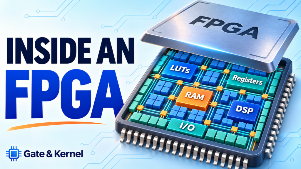
An FPGA, or Field-Programmable Gate Array, contains configurable logic, storage resources, specialized arithmetic circuits, and programmable connections. These building blocks allow designers to create digital circuits for tasks such as controlling equipment, processing signals, and communicating with other devices.
The physical resources are manufactured into the chip. Configuring an FPGA determines how those resources behave and how they connect. The same device can therefore implement different circuits without changing its silicon.
To understand what is inside an FPGA, we can begin with its main building blocks and see how they work together.
1. Inside an FPGA
The configurable part of an FPGA is often called the FPGA fabric. It consists of many small logic blocks connected through a programmable routing network. Dedicated memory, arithmetic, clocking, and input/output resources support this fabric.
Rather than imagining an FPGA as a collection of CPU cores, think of it as a collection of digital building blocks. A designer combines these blocks to create counters, controllers, data-processing pipelines, communication interfaces, and other circuits.
Different FPGA families provide different combinations of resources. Some devices also include built-in processors, high-speed transceivers, or specialized controllers. These are additional capabilities; the central idea remains configurable hardware connected by programmable interconnects. AMD’s architecture documentation, for example, identifies LUTs, registers, memory, DSP blocks, I/O, and routing as major resources.
2. LUTs and Registers
Two important components inside an FPGA’s logic blocks are lookup tables, usually called LUTs, and registers. They perform different but complementary jobs.
LUTs: Implementing Logic Functions
A LUT implements a logic function by storing the output associated with each possible combination of inputs. The input signals select which stored result appears at the output.
For example, a LUT can implement an AND function, where the output is one only when both inputs are one. Changing its configuration allows the same LUT hardware to implement a different function, such as OR or XOR.
This happens directly in hardware. A CPU does not need to execute instructions to look up each result.
A single LUT handles a limited number of inputs. Larger functions are built by combining multiple LUTs and other available resources. We will examine LUT operation and truth tables more closely in a separate article.
Registers: Holding Data and State
A register stores a value. In FPGA logic, registers are commonly built from flip-flops, with each flip-flop storing one bit.
In a typical synchronous circuit, a register captures its input on a selected clock edge and holds that value until a later update. Registers can store a counter value, remember a controller’s current state, or hold intermediate results between processing stages.
The distinction is straightforward: LUTs produce logic results, while registers preserve data and state. A LUT output can feed a register, or it can connect to other logic without being registered at that point.
FPGA manufacturers group these resources differently. Logic blocks may also include multiplexers, which select between signals, and dedicated carry circuitry for arithmetic. The exact arrangement depends on the device family.
3. Programmable Routing
Logic blocks become useful when they are connected. Programmable routing provides the signal paths between LUTs, registers, memory blocks, DSP blocks, and I/O resources.
The chip already contains physical wires and configurable connection points. During implementation, FPGA design tools select paths that connect the resources required by the design.
For example, a counter needs connections between the logic that calculates its next value and the registers that store its current value. A communication circuit needs paths between input pins, control logic, and data buffers.
Routing also affects performance. Signals take time to travel through wires and switches, so the placement of resources and the paths between them influence how quickly a circuit can operate.
This is why FPGA design involves both placement, which assigns functions to physical resources, and routing, which connects them.
4. Block RAM
Registers are useful for holding individual values and small amounts of state. Larger data buffers often benefit from dedicated memory resources called Block RAM, or BRAM.
Block RAM is memory built into the FPGA. It can hold incoming data, stored samples, lookup data, or information waiting to be processed. Using dedicated memory can avoid consuming large numbers of general-purpose logic resources.
A common application is a FIFO, meaning First In, First Out. A FIFO stores data in the order it arrives and releases it in the same order. It helps manage temporary differences between the rate at which one circuit produces data and another circuit consumes it.
Many Block RAM resources provide two access ports, although the supported operations and read/write behavior depend on the device and configuration.
Some FPGAs also allow certain LUTs to act as small memories, often called distributed RAM. Dedicated Block RAM and LUT-based memory offer different tradeoffs in capacity, placement, and access behavior.
Block RAM capacity is limited. A design that needs much more storage may connect to external memory, such as DDR memory, through an appropriate controller and interface.
5. DSP Blocks
Many FPGAs contain dedicated Digital Signal Processing blocks, usually called DSP blocks or DSP slices. These provide arithmetic hardware for operations such as multiplication and addition.
One common operation is multiply-accumulate: multiply two values and add the product to an accumulated result. This operation appears frequently in digital filters, audio processing, image processing, and other numerical workloads.
Such calculations can also be implemented using general-purpose logic. However, dedicated DSP resources can reduce the amount of LUT-based logic required and improve performance or efficiency for suitable operations.
A DSP block is not necessarily a complete DSP processor running software. It is a hardware arithmetic resource that can be configured and connected to other parts of the FPGA.
The supported number formats, operand widths, and arithmetic modes vary between FPGA families. The design tools can map suitable arithmetic descriptions onto these resources.
6. I/O and Clock Resources
An FPGA needs both a way to communicate with the outside world and a way to coordinate its synchronous circuits.
I/O: Connecting to External Devices
I/O stands for Input/Output. I/O resources connect internal FPGA signals to package pins and, through the circuit board, to external components.
Inputs might come from switches, digital sensors, or another chip. Outputs might control LEDs, send data to a display, or communicate with external equipment.
I/O configuration includes more than selecting whether a pin is an input or output. The design must also use electrical standards and voltage levels supported by the FPGA and the connected hardware.
Pins are commonly organized into I/O banks that share certain electrical constraints. Pin assignments and bank voltages therefore need to match the board design.
An ordinary digital I/O pin does not directly measure an analog signal. An analog sensor generally needs an analog-to-digital converter, either external or built into a device that provides that capability.
Clock Resources: Coordinating Updates
A clock provides a timing reference for synchronous logic. Registers use clock edges to determine when to capture new values.
FPGAs include dedicated clock distribution networks designed to deliver clock signals across the chip with controlled timing differences. Many devices also provide clock-management circuits, such as phase-locked loops, or PLLs, for generating related clock frequencies and adjusting timing.
Not every circuit in an FPGA must use the same clock. However, transferring data between different clock domains requires careful design to keep communication reliable.
7. Putting It All Together
Consider an FPGA that receives digital samples from an external sensor interface, processes them, and sends the results to another device.
The samples first enter through I/O resources. Logic built from LUTs and registers controls when data is accepted and tracks the interface’s operating state. Block RAM can buffer samples while they wait for processing.
DSP blocks can perform the multiplications and additions required by a digital filter. Registers hold intermediate results between processing stages. Programmable routing connects these resources, while clock networks coordinate the synchronous parts of the circuit.
Finally, an output interface sends the processed data through the appropriate I/O pins.
These activities can overlap. While one sample is being processed, another can enter a buffer and an earlier result can leave the FPGA. This is possible when the design provides the necessary hardware and organizes it to work concurrently.
Not every design needs every resource. A simple LED controller may use only a small amount of logic, registers, routing, and I/O. A signal-processing system may use substantial memory and many DSP blocks.
Conclusion
An FPGA combines configurable logic with storage, arithmetic, routing, and interface resources. LUTs implement logic functions, registers hold state, routing connects the circuit, Block RAM stores data, DSP blocks perform arithmetic, and I/O resources connect the design to external hardware. Clock resources support coordinated operation.
Understanding these building blocks makes an FPGA easier to understand as a complete system. Its flexibility comes from configuring existing hardware resources and connecting them to perform a particular task.
The next article will take a closer look at LUTs: how a small table of stored output values can implement different digital logic functions.