Combinational logic refers to logic circuits where the output is determined solely by the current input values. Combinational logic circuits can be constructed from simple logic gates like AND, OR, NOT gates, etc., combined in various ways to produce complex logic circuits that perform various logical operations.
Boolean Algebra is a mathematical system used to analyze and simplify logic circuits. It consists of three basic operations: AND, OR, and NOT, which are used to construct complex expressions that represent the operation of a logic circuit.
AND operation takes two input signals and produces an output signal that is high only when both input signals are high. The symbol used for the AND operation is ‘&’.
OR operation takes two input signals and produces an output signal that is high when either or both input signals are high. The symbol used for the OR operation is ‘|’.
NOT operation takes one input signal and produces an output signal that is the inverse of the input signal. The symbol used for the NOT operation is ‘~’.
In learning about AND and OR logic, multiple combinations have already been mentioned, such as Y=ABCD, Y=A+B+C+D, etc. However, in Boolean algebra, not only can these simple combinational operations be completed, they can also be combined with each other. For example, the combination of “AND” and “NOT” forms NAND logic, the combination of “AND” and “OR” forms AND-OR logic, and the combination of “OR” and “NOT” forms NOR logic.
These combined logics can be further combined to form extremely complex combinational logic operations, such as Y=AB+CD. Of course, these complex combinational logics also follow specific mathematical rules during calculation, such as operation priority, calculation order (such as from left to right), commutative law, associative law, distributive law, etc. After learning about logic symbols, truth tables, and logic functions, these three more professional methods will be introduced to you for combinational logic design.
1.NAND Logic Operation
The combination of “AND” and “NOT” forms the NAND logic operation. NAND operation is a combination of the AND and NOT operations (NOT AND), where the output of the AND gate is fed into the input of the NOT gate. The output of the NAND gate is low only when both input signals are high.
1.1) The Logical NAND Gate Functions :
Y=~(A&B)
Y=!(A&B)
Y=AB in Digital Circuit
Y=A.B in Digital Circuit
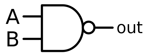
1.2) The Logical NAND Gate Symbols:
The logical symbols for NAND are shown below:
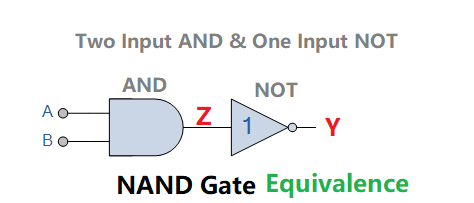
1.3) The Logic NAND Gate Equivalence
For the NAND operation, it can also be done in two steps, as Q = ~(A&B). first, Z = A&B, second, Y = ~Z. As shown below,
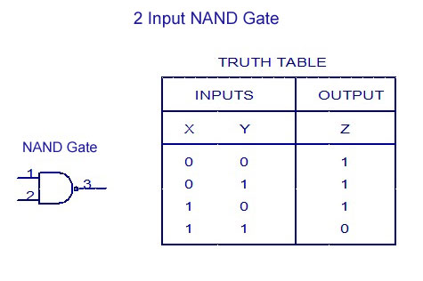
1.4) The Logic NAND Gate Truth Table
2 Input NAND gate truth table is shown in below.
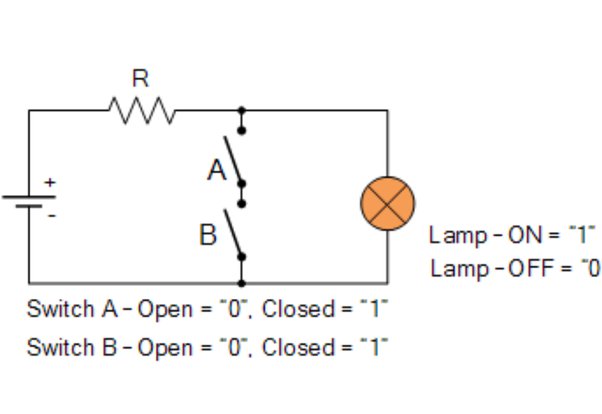
1.5) The Logic NAND Switch Representation
Note:
Since the priority of “NOT” is higher than “AND” in the combined operation of “AND-NOT”, in order to express it correctly, parentheses should be added where necessary, such as Y = ~(A&B) and Y = ~A&B have different meanings; the meaning of Y = ~A&B is to take the NOT of A first and then AND it with B.
2. NOR Logical Operation
NOR operation is a combination of the OR and NOT operations (NOT OR), where the output of the OR gate is fed into the input of the NOT gate. The output of the NOR gate is high only when both input signals are low.
2.1)The Logical NOR Gate Functions:
Y=~(A|B)
Y=!(A|B)
Y=A+B In Digital Circuit
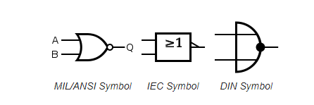
2.2) The Logical NOR Gate Symbols:
There are three symbols for NOR gates: the American (ANSI or ‘military’) symbol and the IEC (‘European’ or ‘rectangular’) symbol, as well as the deprecated DIN symbol. For more information see Logic Gate Symbols. The ANSI symbol for the NOR gate is a standard OR gate with an inversion bubble connected. The bubble indicates that the function of the or gate has been inverted.
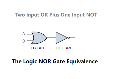
2.3) The Logic NOR Gate Equivalence
the NOR operation can also be seen as a two-step operation, which first performs an OR operation between A and B, and then negates the result.
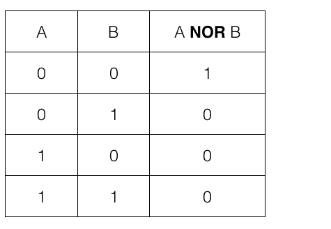
2.4) The Logic NOR Gate Truth Table
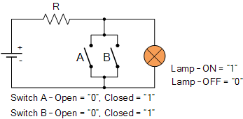
2.5) Logical NOR Switch Representation
The truth table for the NOR function is the opposite of that for the previous OR function because the NOR gate performs the reverse operation of the OR gate. Then we can see that the NOR gate is the complement of the OR gate.
3. OR-AND Logical Operation
OR-AND operation refers to a logical expression on the right side of an assignment statement that contains both OR and AND logic, with OR being evaluated first and then AND.
For example, in the logic function Y=(A+B)(C+D), the expression (A+B)(C+D) is evaluated first by computing A+B and C+D, and then by performing AND between the two. As AND logic has higher precedence than OR logic, the parentheses in Y=(A+B)(C+D) cannot be omitted. The logic symbols for this operation are shown in Following Figure
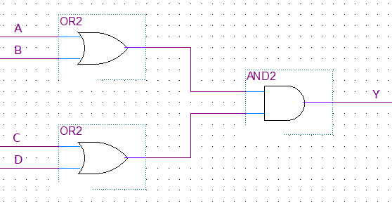
Because the OR-AND operation is a conventional design, there is no specific symbol prescribed for it, and it is directly designed by combining the symbols of OR gate and AND gate circuits.
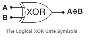
4. XOR Logical Operation
XOR logic operation, also known as “exclusive or operation”, refers to a logic operation that outputs true when the logic values of the two inputs are different, and false when they are the same. Its logic symbol is “⊕”, or written as “xor”. The XOR logic operation can be used in fields such as data encryption and verification.
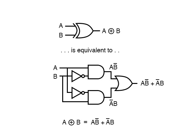
4.1) Logical XOR Functions
Y=AB + AB =A⊕B –in Digital Circuit
Y =(~A)B|A(~B) = ~AB|A~B =A^B –in Verilog or System Verilog
In digital circuits, the symbol “⊕” is used to represent the XOR operation, while in Verilog or System Verilog, the symbol "^" is used.
From the expression ~AB|A~B, it can be seen that the “not” operation has a higher priority than the “and” and “or” operations, so the parentheses can be omitted.
4.2) The Logical XOR Gate Symbols
4.3) The Logic NOR Gate Equivalence
4.4) The Logic NOR Gate Truth Table
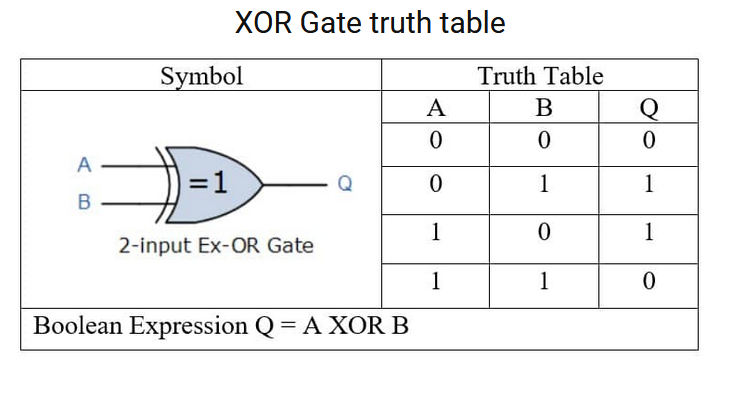
The truth table shows that Q is 1 only when the values of A and B are different, and it is 0 otherwise.
4.5 Logic circuit symbols generated according to the logic function Y =(~A)B|A(~B) = ~AB|A~B
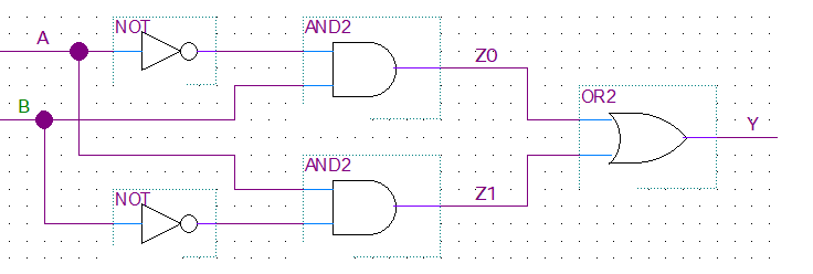
The XOR circuit composed of AND, OR, and NOT is a logic circuit based on NOR and NAND gates used to implement the XOR operation. The circuit typically consists of two inputs and one output. The implementation is as follows:
- Input A and B are separately fed into two NOR gates to obtain the results of NOR(A, B) and NOR(~A, ~B).
- The results of NOR(A, B) and NOR(~A, ~B) are then fed into a NAND gate to obtain the XOR result Y.
The truth table of this circuit is the same as that of the XOR logic, where only when A and B are different, the output Y is 1; otherwise, the output is 0.
The XOR logic can be used to implement one-bit addition because the truth table for XOR operation is the same as that for one-bit addition.
5. NXOR Logical Operation
NXOR, short for “Not XOR,” is a logical operation that outputs a true (1) value if both of its inputs are either both true or both false. In other words, NXOR returns the opposite of the output of the XOR operation.
5.1)XNOR Gate Symbol and Truth Table
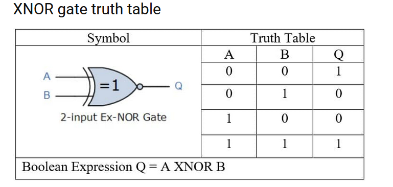
5.2 ) XNOR Gate Truth Table
For example, consider the truth table of the NXOR operation:
| Input A | Input B | Output |
|---|---|---|
| 0 | 0 | 1 |
| 0 | 1 | 0 |
| 1 | 0 | 0 |
| 1 | 1 | 1 |
As you can see, the output is true (1) only when both inputs are the same, either both true or both false. This is the opposite of the XOR operation’s output.
The NXOR operation is also known as the XNOR operation and can be denoted by several symbols, including “⊙”, “≡”, and “↔”. It is used in digital circuits for various applications, including digital signal processing, error detection, and parity checking.
Combinational logic circuits can be designed using logic gates and Boolean expressions. The output of a combinational logic circuit depends only on the current input values and does not depend on any previous input values or the current state of the circuit.
In summary, combinational logic circuits are constructed from basic logic gates and can perform various logical operations using Boolean algebra. The output of a combinational logic circuit depends only on the current input values and not on any previous input values or the current state of the circuit.