The basic logical operations of Boolean algebra are also composed of the basic operations of “AND”, “OR”, and “NOT”.
These three basic operations are combined to form “NAND”, “NOR”, “XNOR”, “XOR”, and other operations. Definitions for each logical operation are provided for Boolean algebra variables and logical equations.
1. Logical AND
Definition: The event (Y) can only occur when all the conditions (A, B, C, etc.) that determine the event (Y) have been met.
The expression is:
Y = A & B & C ... or Y = ABC...
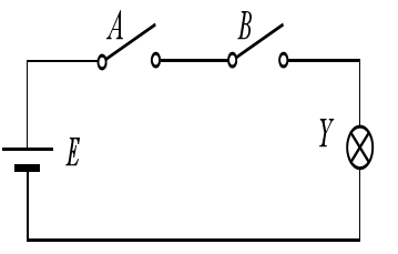
Example 1.1:
Switches A and B are connected in series to control the light bulb Y, where the definitions are as follows:
- The values of A and B are 1 when the switches are closed and 0 when they are open.
- The value of Y is 1 when the light bulb is on and 0 when it is off.
- The value of Y is only 1 when both A and B are 1, and it is 0 for all other cases.

From a mathematical perspective, Figure 2 provides an abstract description of the relationship between Y and A, B.
Since all possible logical values of A and B have been enumerated and their corresponding logical results on Y are shown, the table provides a complete description of the truth and false (or 1 and 0). Therefore, we call it a truth table. Figure 2 is a truth table for logical AND.
1.2 Logical Symbols of AND
The circuit that implements the logical AND operation is called an AND gate. The logical symbol for an AND gate is shown in Figure 3.
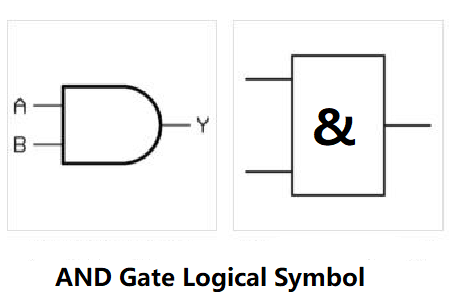
Figure 3 shows the basic symbols that will be used for digital logic diagram design. The symbols on the left are the American and IEEE standard symbols, while those on the right are the international standard symbols of IEC. Currently, both have a relatively large customer base.
1.3 AND Logical Equations
Y = A & B the logical expression for AND operation in computer languages such as Verilog and System Verilog.
Y = A*B is the multiplication expression for AND operation in digital circuits.
Y = AB is the shorthand expression for AND operation in digital circuits.
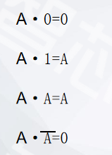
1.4 Some Simple Formulas for Logical AND Operation
1.5 Cascade of Logical AND Operations
Connecting multiple AND gates in series to perform more complex logic operations. The output of one AND gate is connected to the input of the next AND gate in the series. This is often used in digital circuits to implement more complex logical functions.
Example 1.5.1
Y=ABC
2. Logical OR
Definition: the event (Y) occurs if any one or more of the conditions (A, B, C, …) that are necessary for the event to occur are met.
The expression for logical OR :
Y = A + B + C + ...
Example 2.1
Switches A and B control the light bulb Y in parallel. The definition for A and B are as follows:
- The value of A and B is 1 when the switch is closed and 0 when it is open.
- The value of Y is 1 when the light bulb is on and 0 when it is off.
- The value of Y is 1 when either A or B or both are 1, and 0 in all other cases.

Figure 5 describes the function between Y and A, B.
Figure 6 abstractly describes the relationship between Y and A, B from a mathematical perspective.
Because Y enumerates the logical values of all possible combinations of A and B, and their logical effects on Y, the entire table describes the truth values (or 1s and 0s).
Therefore, we call it a truth table. Figre 6 is the truth table for the logical OR.
2.2 Logical Symbols of OR
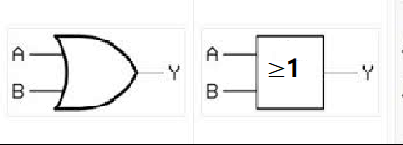
Implementing the logical circuit of OR is called OR gate. The logical symbols of the OR gate are designed as shown in Figure 7, with the left side being the ANSI/IEEE symbol and the right side being the IEC international symbol.
2.3 OR Logical Equations
Y=A|B
Y=A+B shorthand expression for OR operation in digital circuits.
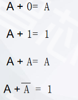
2.4 Some Simple Formulas for Logical OR Operation
2.5. Cascade of Logical OR Operations
The above introduces 2-input OR logic, OR logic can also perform multi-input operations, such as:
Y=A+B+C
3. Logical NOT
If the condition (A) for an event (Y) is satisfied, the event (Y) will not occur.
Expression:
Y=Ā


Example 3.1
In Figure 9 circuit diagram. Switch A controls light bulb Y, with the following definitions:
- The value of A is 1 when the switch is closed, and 0 when it is open.
- The value of Y is 1 when the light bulb is on, and 0 when it is off.
- The value of Y is 1 only when A is 0, otherwise it is 0.
- The truth table are shown in figure 10.
3.2 Logical Symbols of NOT
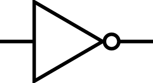
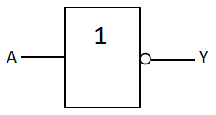
The circuit that implements the NOT logic is called a NOT gate. The logic symbol of a NOT gate is shown in Figures 11 and 12.
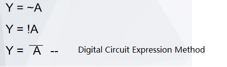
3.3 NOT Logical Equations
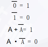
3.4 Some Simple Formulas for Logical NOT Operation
Logical NOT is the operation of negating the input logic variable and assigning it to the output variable.