In the previous class, we introduced the entrance and behavioral description of logic circuits in Verilog. The syntax rules are very simple, essentially a textual description of digital circuits. This means that a single circuit in a digital circuit can be described using this method. However, in digital circuit design, complex circuits are often implemented by multiple sub-circuits or devices. How does Verilog correspond to this?
In the Verilog structure, hierarchy can be implemented through instantiation. In this class, we will design a 1-bit full adder and instantiate it, and then use it as an example to show how to achieve hierarchical circuit design through instantiation in a 4-bit full adder. The purpose of instantiation is to use a completed design as a sub-design or submodule, and to fully utilize the results of the design for design accumulation.
In Verilog design, although there may be multiple modules, only one module’s ports are responsible for the input and output of the entire design architecture. If an internal module has inputs and outputs, they interact with the external circuit through port mapping after instantiation.
Before the formal design, let me introduce a few logical operators.
1. Logical Operators
Logical operators are fundamental to Verilog code. The logical operators that are built into Verilog are:
- Logical AND operator is represented by the symbols ‘and’ and ‘&’
- Logical OR operator is represented by the symbols ‘or’ and ‘|’
- Logical XOR (Exclusive OR) operator operator is represented by the symbols ‘xor’ and ‘^’
- Logical NOT operator is represented by the symbols ‘!’
- Logical Inverse operator is represented by the symbols ‘~’
- Parallel Bit Operators is represented by the symbols ‘{}’
To put it simply, it means combining multiple bits in a cascading manner to form a new variable. For example, a and b are single variables, whereas y[1:0] is a vector.
Assign y={a,b};
Results:
y[0]=b, y[1]=a;
The main purpose of the operators referenced here is to help the understanding of the operators used in the design of this section, please refer to the verilog operators for details.
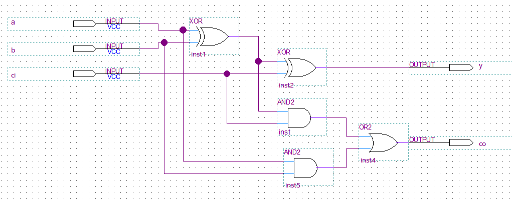
2. Design of 1-bit full adder
Inputs: a, b ,ci; where ci is Carry input
| Input Variables | Output Variables | |||
| a | b | ci | y | co |
| 0 | 0 | 0 | 0 | 0 |
| 0 | 0 | 1 | 1 | 0 |
| 0 | 1 | 0 | 1 | 0 |
| 0 | 1 | 1 | 0 | 1 |
| 1 | 0 | 0 | 1 | 0 |
| 1 | 0 | 1 | 0 | 1 |
| 1 | 1 | 0 | 0 | 1 |
| 1 | 1 | 1 | 1 | 1 |
The following logical expressions can be obtained from the truth table:
y=a xor b xor c;
co=(~a&b & ci) | (a &~b& ci) | ( a & b&~ci) | ( a & b & ci) = ci & (a xor b) | (a & b);
 One full adder Verilog description. When storing the file, store it with a .v extension, e.g. fadder1.v, and store it with the same name as the module name (in this case, fadder1).
module fadder1
(
    input ci,
    input a,
    input b,
    output y,
    output co
);

assign y=a ^ b ^ ci;
assign co=ci&(a ^ b) | a&b;

endmodule
3. Design of 4-bit full adder
In A new file, the verilog codes of 4-bit full adder are as following:
module fadder4
(
    input ci,
    input  [3:0] a,
    input  [3:0] b,
    output [3:0] y,
    output co
);

wire co1,co2,co3;

//  Instantiation one bit full adder, duplicated four times
fadder1 fadder1_inst1
(
  .ci (ci),
  .a (a[0]),
  .b (b[0]),
  .y (y[0]),
  .co (co1)
);

fadder1 fadder1_inst2
(
  .ci (co1),
  .a (a[1]),
  .b (b[1]),
  .y (y[1]),
  .co (co2)
);

fadder1 fadder1_inst3
(
  .ci (co2),
  .a (a[2]),
  .b (b[2]),
  .y (y[2]),
  .co (co3)
);

fadder1 fadder1_inst4
(
  .ci (co3),
  .a (a[3]),
  .b (b[3]),
  .y (y[3]),
  .co (co) //map the ports defined in this module to the ports in the lower-level module, and you can use the same name.

);

endmodule
The format for module instantiation is as follows:
Module Name Instance Name
(
...
);
The instance name can be named freely, it doesn’t have to be the same as the module name, but it is often given a meaningful name when used to increase the readability of the code.
( … ) includes port mapping, such as connecting co3 to the ci of the original 1-bit full adder in fadder1_inst4 through .ci(co3) to establish a named association. This association method is called named association. That is, the design module and the instantiation module are associated with each other by name.
In named association, the ports in the instantiation module do not need to be arranged in the same order as in the instantiation module.
fadder1 fadder1_inst4

(

  .ci (c03),

  .a (a[3]),

  .b (b[3]),

  .y (y[3]),

  .co (co)

);
Named association does not require the ports in the instantiation module to be arranged in the same order as in the design module. For example, the instantiation usage below has the same effect as the previous one:
fadder1 fadder1_inst4

(

  .ci (c03),

  .b (b[3]),

  .a (a[3]),

  .co (co),

  .y (y[3])

);
Another way of instantiation is positional correspondence, for example:
fadder1 fadder1_inst4

(

  c03,

  a[3],

  b[3],

  y[3],

  co

);
When using the instance, connect the ports strictly according to the order defined in the module, without specifying the port names specified in the original module definition. Since the port order of module fadder1 is ci, a, b, y, co when defined, the corresponding relationship in the position-related instantiation above is co3 <–> ci, a[3] <–> a, b[3] <–> b, y[3] <–> y, co <–> co.
Generally in the case, the name association is used most often.