FPGA (Field Programmable Gate Array) is a programmable digital logic device with wide applications such as digital signal processing, image processing, communication, and networking. FPGA has various input/output interfaces, among which bidirectional I/O is a special interface that can both input and output data.
The bidirectional port is usually implemented by an I/O pin, and its input and output states can be set by the program. When using a bidirectional port, special attention needs to be paid to the data direction and data validity. Additionally, a control signal needs to be set to switch the data direction.
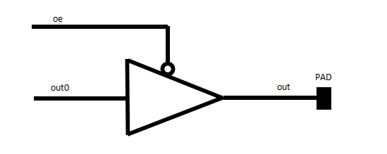
The bidirectional port of FPGA is widely used in FPGA design applications, such as SDA in I2C interface, data line in 3-wire SPI interface, data bus in traditional control bus, and data bus for accessing DDR3/DDR4 memory, etc. Bidirectional access involves many concepts, such as the concept of tristate, high-impedance, input/output pin merging, input/output time-division multiplexing, etc. Therefore, beginners are often confused and feel at a loss. This article starts from the basic principles of the underlying hardware and reveals the mechanism of bidirectional ports. Using Verilog program development as an example, it guides readers step by step on how to use and develop bidirectional ports (inout).