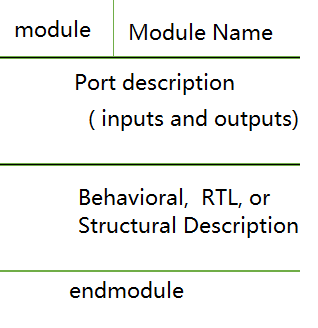
A module is the most basic syntax structure in the Verilog language. It can not only describe logical behavior within the module, but also serves as the interface between Verilog behavioral structure descriptions and external circuits. It can be said that in Verilog synthesizable development, other structures or functional structures are optional, but the module is the only one that must exist.
The structure described by the module is more like a complete digital circuit, with a name, inputs, outputs, and logical behavior.
Its structural diagram is shown in the following figure.
Port description in English refers to the declaration of the inputs and outputs of a Verilog module. Ports serve as the interface between a module and other modules or external circuits, and allow data to be transferred in and out of the module. The port declaration specifies the name, direction (input or output), and size (number of bits) of each port. For example, a port declaration might include “input [7:0] data_in” to indicate that the module has an 8-bit input port called “data_in”.
Behavioral, RTL, or Structural Description refer to different methods of describing a digital circuit using the Verilog hardware description language.
- Behavioral description describes the circuit’s functionality using high-level language constructs, without specifying how the circuit is implemented.
- RTL (Register-Transfer Level) description describes the circuit in terms of the flow of data between registers and the logic that manipulates that data.
- Structural description describes the circuit in terms of the specific gates, flip-flops, and other hardware components that make up the circuit.
All three types of descriptions are used to model and simulate digital circuits in Verilog, with each having its own advantages and disadvantages depending on the specific application.
1. The Syntax Structure of a Module
The syntax structure of a module in Verilog consists of the following elements:
- The keyword
modulefollowed by the name of the module. - The port list, enclosed in parentheses and consisting of the input and output ports declared using the keywords
inputandoutput, respectively. Each port declaration specifies the port name, size (number of bits), and optional direction (reg,wire,output reg, etc.). - The module body, enclosed in curly braces and consisting of the declarations and statements that define the behavior of the module. This can include assignments, conditional statements, loops, and calls to other modules.
1.1 Example
Here’s an example of a simple Verilog module:
module adder(input [7:0] a, input [7:0] b, output [8:0] sum);
  reg [8:0] temp_sum;

  always @(*) begin
    temp_sum = a + b;
    sum = temp_sum;
  end
endmodule
This module takes two 8-bit inputs a and b, adds them together, and outputs the 9-bit sum sum. The module body contains an always block that assigns the sum to a temporary register temp_sum, which is then assigned to the output port sum.
1.2 Port: defines input (input), output (output), or bidirectional (inout)
The input keyword is used to define a port that receives data from external sources into the module, the output keyword is used to define a port that sends data from the module to external components, and the inout keyword is used to define a port that can both send and receive data. Each port is associated with a specific signal or group of signals and may have a specified width or number of bits.
( input a,

input b,

output c   //last port,no comma ","

);
1.3 the Behavioral Description Section
Used to describe the behavior of the digital logic. For example, assign c = a & b; represents the logical relationship between c, a, and b, where c is assigned the logical value resulting from the AND operation between a and b.
assign is used to indicate a subsequent assignment statement. The module definition ends with the endmodule keyword.
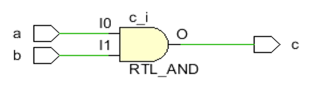
1.4 and-gate Example
module and_gate

  (  input a,

     input b,

     output c

  );

assign c =a & b;

endmodule
The equivalent digital circuit is shown below:
The input and output ports can be represented using vectors. For example, the 4 input ports a[3:0] and the 4 input ports b[3:0] can be ANDed pairwise, and the resulting values are assigned to the corresponding output ports c[2:0].
1.5 and4 Example
Verilog descriptive methods:
module and4

(

  input   a0,a1,a2,a3,

  input   b0,b1,b2,b3,

  output  c0,c1,c2,c3


);

assign  c0=a0 & b0;

assign  c1=a1&b1;

assign  c2=a2&b2;

assign  c3=a3&b3;

endmodule
The code can be rewritten using vectors as follows:
module and4

(

  input   [3:0] a,

  input   [3:0] b,

  output  [3:0] c

);


assign  c[0]=a[0]&b[0];

assign  c[1]=a[1]&b[1];

assign  c[2]=a[2]&b[2];

assign  c[3]=a[3]&b[3];

endmodule
In the above program, a 4-bit input a is defined using vectors. When using a, it can be used either as a whole vector or as individual bits. When indexing, the index number is typically represented within square brackets [], such as a[0] represents the first variable in the array, and a[3] represents the fourth variable. A range of variables can also be referenced, such as a[2:1], which uses a[2] and a[1]. If the vector is used as a whole, it is represented as a[3:0], or directly as a. Because vectors can be operated on bitwise or used individually, they are more flexible and convenient than arrays defined in computer software programming.
Since the & operator performs a bitwise AND operation, it can also be implemented using the following code:
module and4

(

  input   [3:0] a,

  input   [3:0] b,

  output  [3:0] c

);

assign  c=a & b;//按照位的顺序,逐位相与

endmodule
“The usage of ports defined with input and output is relatively simple. In future courses, we will further explore knowledge related to FPGA and ASIC hardware, such as voltage levels, rise and fall times, pull-up and pull-down resistors, as well as the usage of interfaces such as DDR and LVDS.
The usage of inout ports, which are defined as bidirectional, is more complex, and we will have a dedicated section to discuss it in a later chapter.”