Introduction
Semiconductor yield is a measure of how many chips manufactured during a production process meet the required quality and functional specifications.
It is one of the most important indicators of semiconductor manufacturing efficiency, cost, and reliability.
Modern semiconductor fabrication facilities, commonly called fabs, manufacture hundreds or thousands of integrated circuits on a single silicon wafer.
However, not every fabricated chip functions correctly.
Manufacturing defects, process variations, and design-related problems can cause some chips to fail testing.
Yield measures the proportion of usable products produced during manufacturing.
It directly affects the cost of CPUs, GPUs, memory chips, microcontrollers, FPGAs, ASICs, and other semiconductor devices.
How Does Semiconductor Yield Work?
Semiconductor manufacturing involves hundreds or thousands of processing operations, including photolithography, deposition, etching, ion implantation, and metallization.
During these operations, tiny defects or manufacturing variations may affect the electrical behavior of individual circuits.
For example, a defect in a metal interconnection may cause an open circuit, while an unwanted conductive connection may create a short circuit.
After fabrication, chips are electrically tested to determine whether they satisfy the required specifications.
The number of functional chips is compared with the total number of fabricated chips to calculate yield.
A higher yield means more usable products are obtained from the manufacturing process.
How Is Die Yield Calculated?
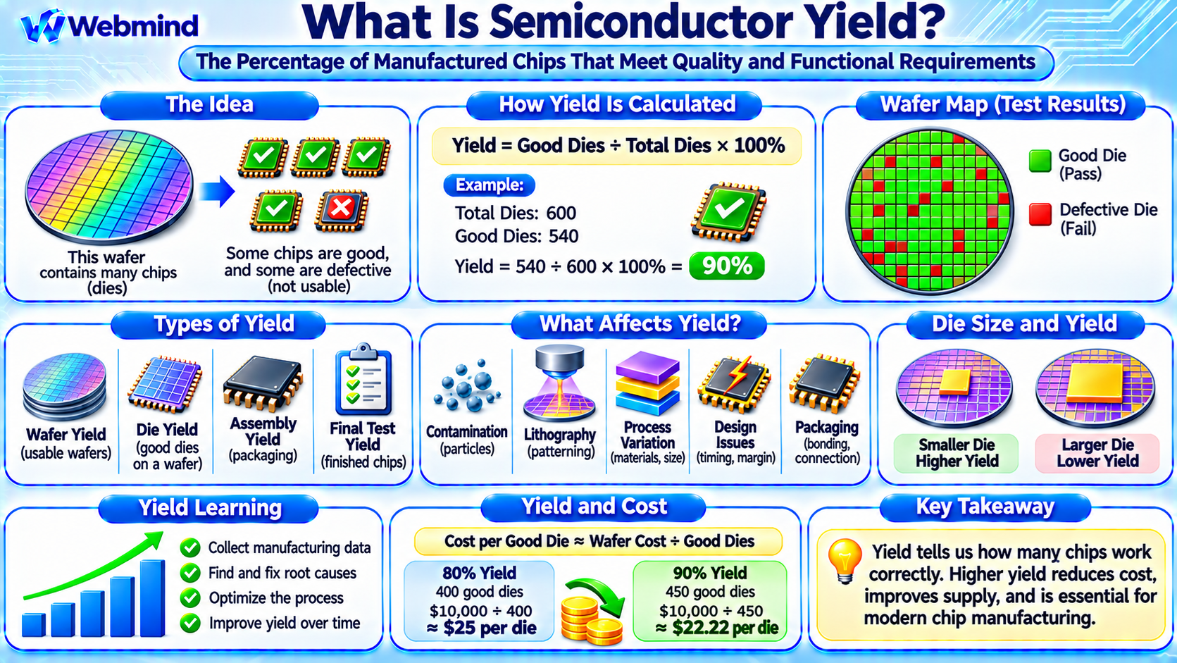
Die yield measures the proportion of complete semiconductor dies that pass the required tests.
The basic formula is:
Die Yield = Good Dies ÷ Total Dies × 100%
For example, suppose a silicon wafer contains 600 complete dies.
If 540 dies pass testing, the yield is:
Die Yield = 540 ÷ 600 × 100% = 90%
This means that 90 percent of the fabricated dies are classified as functional according to the selected test criteria.
The remaining 10 percent may contain defects or fail to meet the required specifications.
In practice, semiconductor manufacturers use more detailed yield metrics to distinguish manufacturing defects, electrical performance, and other quality requirements.
What Are the Main Types of Semiconductor Yield?
Semiconductor manufacturing uses several yield measurements.
Wafer Yield
Wafer yield measures the proportion of wafers that successfully complete a manufacturing process and meet the required criteria.
A wafer may be rejected because of severe defects, equipment problems, or manufacturing failures.
Die Yield
Die yield measures the proportion of complete dies on a wafer that pass electrical or functional testing.
This is one of the most commonly discussed semiconductor yield metrics.
Assembly Yield
Assembly yield measures the proportion of semiconductor devices that successfully complete packaging and assembly operations.
Problems such as damaged dies, defective electrical connections, or bonding failures can reduce assembly yield.
Final Test Yield
Final test yield measures the proportion of packaged devices that pass the required electrical, functional, and performance tests.
A chip may pass wafer-level testing but fail after packaging because of assembly damage or other problems.
Overall Manufacturing Yield
Overall yield reflects the combined effect of multiple manufacturing stages.
When stage yields are defined on a consistent population and measured sequentially, overall yield can be calculated by multiplying the individual stage yield fractions.
For example, if wafer fabrication produces a 90% die yield, assembly yield is 98%, and final test yield is 99%, the combined yield is approximately 87.3%.
What Causes Semiconductor Yield Loss?
Several factors can reduce semiconductor manufacturing yield.
Particle Contamination: Tiny particles can interfere with lithography, deposition, or etching processes and damage microscopic structures.
Lithography Defects: Patterning errors can produce incorrect transistor or interconnection dimensions.
Process Variation: Differences in temperature, material thickness, doping, or other manufacturing conditions can affect electrical characteristics.
Metal Interconnection Defects: Open circuits, short circuits, and excessive resistance can cause functional failures.
Material Defects: Crystal imperfections or unwanted impurities may affect transistor operation.
Packaging Defects: Poor bonding, damaged connections, or mechanical stress can cause failures after wafer fabrication.
Design-Related Problems: Layout weaknesses, insufficient timing margins, or sensitivity to process variation can reduce the number of chips meeting specifications.
Foundries continuously monitor these factors to improve manufacturing consistency.
What Is Defect Density?
Defect density describes the number of manufacturing defects within a specified semiconductor area.
It is commonly expressed as defects per square centimeter.
Higher defect density generally reduces yield because individual dies have a greater probability of containing a harmful defect.
A simplified Poisson yield model is:
Yield = e^(-D × A)
Where D represents defect density, A represents die area in compatible units, and e is the mathematical constant.
For example, consider a die with an area of 1 cm² and a defect density of 0.1 defects per cm².
The simplified model predicts a yield of approximately 90.5%.
Real manufacturing yield models are more complicated because defects are not always randomly distributed and not every defect causes a chip failure.
Nevertheless, defect density is an important concept in semiconductor manufacturing.
Why Does Die Size Affect Yield?
Larger semiconductor dies generally have a greater probability of containing manufacturing defects.
Suppose two chips are manufactured using the same process technology.
One die occupies 100 mm², while another occupies 400 mm².
The larger die covers four times as much silicon area and therefore has greater exposure to potential defects.
This can reduce the percentage of usable chips obtained from a wafer.
Large dies also reduce the number of complete chips that fit on a wafer.
For these reasons, die area strongly influences manufacturing cost.
However, actual yield depends on defect distribution, circuit layout, redundancy, process maturity, and testing requirements.
Yield and Semiconductor Process Nodes
Advanced semiconductor process nodes introduce new manufacturing challenges.
As transistor structures and interconnections become smaller, manufacturing tolerances become increasingly demanding.
Technologies such as FinFETs and Gate-All-Around Field-Effect Transistors (GAAFETs) require precise control of three-dimensional semiconductor structures.
Advanced EUV lithography also introduces challenges involving photoresist behavior, stochastic defects, pattern fidelity, and process control.
When a new manufacturing process is introduced, yield may initially be lower while engineers identify and correct manufacturing problems.
As the process matures, defect density and process variation may decrease, improving yield.
However, a smaller process node does not automatically mean lower yield. Actual results depend on the maturity and capabilities of the manufacturing process.
What Is Yield Learning?
Yield learning is the process of identifying manufacturing problems and improving production results over time.
Semiconductor manufacturers collect extensive data from fabrication equipment, inspection systems, wafer testing, and final product testing.
Engineers analyze this information to identify recurring defects, equipment problems, and process variations.
For example, if defective dies repeatedly appear in a particular wafer region, engineers may investigate equipment uniformity, contamination, or other localized process conditions.
After identifying the cause, manufacturers can adjust equipment settings, improve cleaning procedures, or modify process conditions.
Yield learning is especially important during the introduction of new semiconductor technologies.
What Is Wafer Mapping?
Wafer mapping is a technique used to display the test results of individual dies across a semiconductor wafer.
Each die is represented according to its location and test classification.
For example, functional dies may be displayed in green, while defective dies appear in red.
The resulting wafer map can reveal patterns that help engineers identify manufacturing problems.
Defects concentrated near the wafer edge may suggest different causes from defects appearing in repeated clusters or straight lines.
Wafer maps are therefore useful for production monitoring, failure analysis, and yield improvement.
Yield vs. Chip Binning
Yield and binning are related but different concepts.
Yield: Measures how many chips meet the selected acceptance criteria.
Binning: Classifies functional chips according to performance, power consumption, operating voltage, or other characteristics.
For example, two processor dies may both function correctly but achieve different maximum operating frequencies.
One may qualify for a higher-performance product, while the other may be sold as a lower-frequency model.
Some semiconductor products also use redundancy or configurable features to disable defective sections while retaining usable functionality.
This allows manufacturers to recover value from certain dies that would otherwise be rejected.
Binning can therefore improve the economic use of manufactured silicon, although it does not eliminate all manufacturing defects.
How Does Yield Affect Chip Cost?
Semiconductor manufacturing cost depends on wafer processing expenses, die area, yield, packaging, testing, and other factors.
A simplified relationship is:
Cost per Good Die ≈ Wafer Cost ÷ Number of Good Dies
For example, suppose a processed wafer costs $10,000 and contains 500 complete dies.
At 80% yield, the wafer produces 400 good dies, giving a simplified fabrication cost of $25 per good die.
At 90% yield, the wafer produces 450 good dies, reducing the simplified fabrication cost to approximately $22.22 per good die.
This example excludes packaging, testing, design, and other expenses.
It illustrates why even a modest improvement in yield can significantly affect semiconductor manufacturing economics.
Yield and Chiplet Technology
Chiplet technology divides a large semiconductor design into multiple smaller dies.
One potential advantage is improved wafer-level yield.
Instead of manufacturing one very large monolithic die, engineers can fabricate smaller compute, memory, or input/output dies separately.
Smaller dies generally have a lower probability of containing manufacturing defects when other conditions are comparable.
Manufacturers can test the individual dies before assembling them into a multi-die package.
However, the complete product still depends on successful assembly and interconnection of all required components.
A chiplet-based design may improve wafer fabrication yield while introducing additional packaging costs and assembly yield losses.
Therefore, the total economic benefit depends on the entire manufacturing process.
Yield in Advanced Packaging
Modern semiconductor products increasingly combine multiple dies, high-bandwidth memory, and advanced interconnection technologies.
Packaging methods such as 2.5D integration, 3D stacking, and hybrid bonding introduce additional manufacturing steps.
For example, an AI accelerator package may contain a compute die and several HBM stacks.
Each component must function correctly, and the package connections must also meet electrical and reliability requirements.
The probability of obtaining a fully functional package depends on the yields of the individual components and the assembly process.
This makes known-good-die testing and advanced packaging inspection increasingly important.
How Do Foundries Improve Yield?
Semiconductor foundries use several techniques to improve manufacturing yield.
Defect Inspection: Identifies particles, patterning errors, and physical defects during production.
Metrology: Measures critical dimensions, layer thicknesses, alignment, and other manufacturing characteristics.
Statistical Process Control: Monitors production data to detect unusual variations and process changes.
Equipment Maintenance: Helps maintain stable fabrication conditions and reduce unexpected defects.
Design for Manufacturability (DFM): Encourages circuit layouts that are more tolerant of manufacturing limitations.
Electrical Testing: Identifies defective dies and provides information for failure analysis.
Process Optimization: Adjusts manufacturing conditions to improve consistency, reliability, and performance.
These methods help foundries increase production efficiency and reduce cost.
Why Is Semiconductor Yield Important?
Yield is important because semiconductor manufacturing requires large investments in equipment, materials, energy, and engineering.
A lower yield means that fewer usable chips are produced from the same manufacturing resources.
This increases production cost and can reduce available product supply.
Yield also affects the economics of new process nodes, advanced processor designs, and chiplet-based architectures.
For manufacturers, improving yield can be as valuable as increasing transistor density or reducing fabrication time.
For customers, better yield can support more competitive chip pricing and more reliable product availability.
Conclusion
Semiconductor yield measures the proportion of manufactured chips that meet required quality and functional specifications.
It is influenced by manufacturing defects, die size, process variation, transistor technology, packaging, and testing.
Important yield concepts include die yield, defect density, wafer mapping, yield learning, binning, and overall manufacturing yield.
Higher yield reduces the effective cost of usable semiconductor devices and improves manufacturing efficiency.
As advanced process nodes and multi-die packaging become more complex, yield management remains one of the most important challenges in semiconductor manufacturing.
Understanding semiconductor yield provides an essential foundation for studying silicon wafers, semiconductor foundries, process nodes, chiplets, advanced packaging, CPU and GPU manufacturing, and the economics of modern chip production.