Introduction
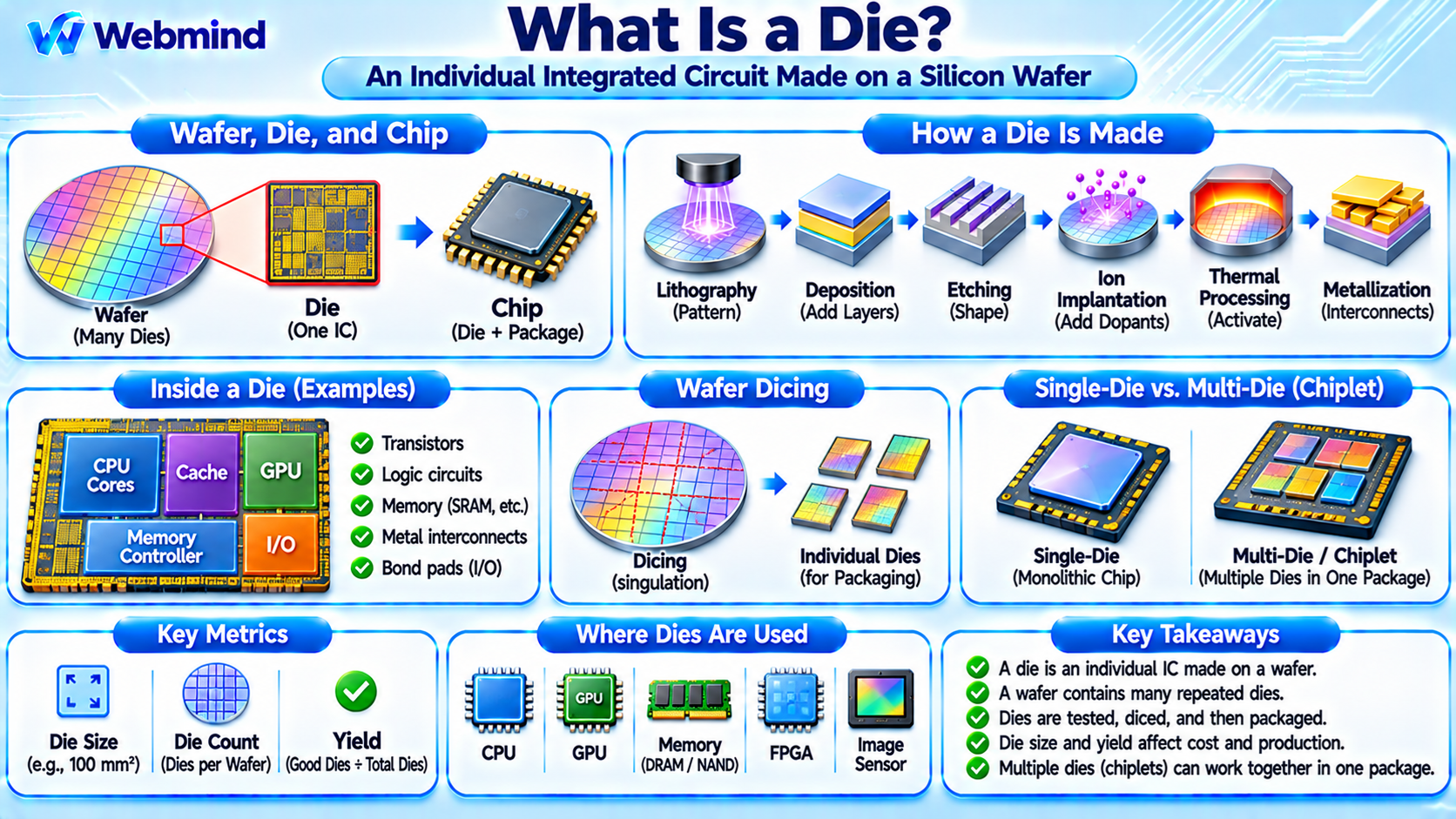
A semiconductor die, also called an integrated circuit die or simply a die, is an individual piece of semiconductor material containing a fabricated electronic circuit.
It is produced on a semiconductor wafer and later separated for packaging and use in electronic devices.
A die may contain millions or billions of transistors, along with metal interconnections, memory structures, and other electronic components.
Semiconductor dies are the foundation of CPUs, GPUs, memory chips, microcontrollers, FPGAs, ASICs, and many other integrated circuits.
Although people often use the terms die and chip interchangeably, a die specifically refers to the semiconductor circuit itself, while a finished chip commonly includes additional packaging and external electrical connections.
How Is a Semiconductor Die Made?
Semiconductor dies are manufactured in large numbers on a silicon wafer.
A wafer is a thin, circular slice of highly purified crystalline silicon.
Modern semiconductor fabrication facilities use processes such as photolithography, deposition, etching, ion implantation, and metallization to build electronic circuits across its surface.
Instead of manufacturing one chip at a time, semiconductor manufacturers create many repeated circuit patterns on a single wafer.
Each individual circuit area becomes a die.
After fabrication, the wafer undergoes electrical testing to identify functional and defective dies.
The wafer is then cut into individual pieces through a process called dicing or singulation.
Suitable dies are transferred to semiconductor packaging operations, where they receive protective structures and electrical connections.
Main Components of a Semiconductor Die
A modern integrated circuit die may contain several important structures.
Transistors: Semiconductor devices that perform switching and amplification. Modern digital processors contain enormous numbers of MOSFET-based transistors.
Logic Circuits: Combinations of transistors implementing operations such as AND, OR, NOT, arithmetic calculations, and control functions.
Memory Structures: Registers, SRAM arrays, and other storage elements used to hold data or processor state.
Metal Interconnects: Multiple layers of conductive wiring that connect transistors and other circuit components.
Insulating Layers: Dielectric materials that electrically separate transistor structures and metal interconnections.
Contact and Via Structures: Conductive connections between semiconductor devices and different wiring layers.
Bond Pads or Die Connections: Structures used to connect the die electrically to its package or neighboring components.
The exact layout depends on whether the die implements a CPU, GPU, memory device, analog circuit, sensor, or another semiconductor function.
Die vs. Wafer vs. Chip: What Is the Difference?
These three terms describe different stages or components of semiconductor manufacturing.
Wafer: A large circular semiconductor substrate containing many fabricated integrated circuits.
Die: An individual integrated circuit formed on the wafer and separated during manufacturing.
Packaged Chip: A semiconductor die, or multiple dies, assembled into a package that provides mechanical protection, electrical connections, and often thermal management.
For example, a processor begins as one circuit pattern among many on a silicon wafer.
After fabrication and testing, the processor die is separated from the wafer and installed in a package.
The finished processor package can then be connected to a computer motherboard.
Thus, the semiconductor die is the functional silicon circuit inside the packaged product.
What Is Die Size?
Die size refers to the physical area occupied by an individual semiconductor die.
It is commonly measured in square millimeters (mm²).
For example, a rectangular die measuring 10 mm by 12 mm has an area of 120 mm².
Die size is influenced by transistor count, manufacturing technology, circuit architecture, cache capacity, input/output interfaces, and other design requirements.
A larger die can contain more circuitry, but it generally increases manufacturing cost and the probability of encountering fabrication defects.
Smaller dies may improve the number of chips obtained from each wafer.
However, die size alone does not determine processor performance. Circuit design, transistor technology, power consumption, and memory architecture are also important.
How Many Dies Can Fit on a Wafer?
The number of dies manufactured on a wafer depends primarily on wafer diameter and die area.
Modern advanced semiconductor manufacturing commonly uses 300 mm wafers.
A smaller die allows more individual circuits to fit on the same wafer, while a larger die reduces the available die count.
However, the number cannot be calculated simply by dividing wafer area by die area.
Because wafers are circular and most dies are rectangular, some space near the wafer edge cannot accommodate complete dies.
Additional space is also required for scribe lines, alignment structures, and manufacturing test features.
The result is commonly called the gross dies per wafer (GDPW), representing the approximate number of complete dies that can be fabricated before accounting for functional yield.
What Is Die Yield?
Die yield describes the proportion of fabricated dies that meet the required quality and functional specifications.
For example, suppose a wafer contains 600 complete dies.
If 540 dies pass the required electrical tests, the simplified functional yield is:
Die Yield = 540 / 600 × 100% = 90%
Several factors influence yield.
Manufacturing Defects: Particles or fabrication imperfections can damage transistor structures or wiring.
Die Area: Larger dies generally have a greater probability of containing defects.
Process Variation: Small variations in transistor dimensions and electrical characteristics can affect performance.
Circuit Design: Layout techniques and fault-tolerant structures can influence how sensitive a design is to manufacturing defects.
Process Maturity: Manufacturing yields often improve as semiconductor processes become better understood and controlled.
Yield is economically important because defective dies consume wafer area and manufacturing resources without becoming fully functional products.
What Is Wafer Dicing?
Wafer dicing is the process of separating individual dies from a completed semiconductor wafer.
Manufacturers typically leave narrow regions called scribe lanes or dicing streets between neighboring dies.
These regions provide space for cutting or separation.
Several techniques are used.
Mechanical Dicing: Uses a high-precision cutting blade to separate dies.
Laser Dicing: Uses laser-based processes to cut or weaken selected regions of the wafer.
Stealth Dicing: Creates internal modified regions in the semiconductor material, allowing controlled separation through subsequent processing.
The method depends on wafer thickness, semiconductor material, die size, and manufacturing requirements.
After separation, individual dies are inspected and transferred to packaging operations.
What Is a Bare Die?
A bare die is an unpackaged semiconductor die.
It contains the fabricated circuit but has not been assembled into a conventional protective semiconductor package.
Bare dies may be used in specialized applications, including advanced packaging, multi-chip modules, and certain compact electronic systems.
For example, a manufacturer may place several bare dies onto a common substrate or interposer to create a larger computing system.
Bare dies require careful handling because their surfaces and electrical connections can be vulnerable to mechanical damage, contamination, and electrostatic discharge.
What Is a Multi-Die Package?
A modern semiconductor package does not always contain only one die.
Some advanced processors combine multiple dies in the same package.
For example, a processor package may contain separate CPU compute dies and an input/output die.
These components communicate through high-speed electrical interconnections inside the package.
This approach can improve manufacturing flexibility and allow different functions to use different semiconductor manufacturing technologies.
A multi-die package may also combine logic chips with high-bandwidth memory or specialized accelerators.
The individual dies remain separate pieces of silicon, but they function together as one packaged computing system.
Die vs. Chiplet: What Is the Difference?
A chiplet is a semiconductor die designed to operate as part of a larger multi-die system.
A traditional monolithic processor integrates its major functional blocks onto one large die.
A chiplet-based design divides selected functions across multiple smaller dies.
For example, one chiplet may contain CPU cores, while another contains memory controllers and input/output interfaces.
These chiplets are connected through advanced packaging technologies.
Chiplet designs can improve manufacturing flexibility, potentially increase yield, and allow different components to use different process nodes.
However, chiplets also introduce challenges involving communication latency, power delivery, thermal management, packaging complexity, and inter-die bandwidth.
Not every die is a chiplet. The term usually refers to a die intentionally designed for integration with other dies in a larger system.
Semiconductor Die Packaging
After wafer dicing, functional dies are commonly assembled into semiconductor packages.
Packaging provides several important functions.
Electrical Connectivity: Connects the die to external circuits through bond wires, solder bumps, redistribution layers, or other structures.
Mechanical Protection: Protects delicate semiconductor circuitry from environmental and physical damage.
Thermal Management: Helps transfer heat away from the operating die.
Signal Integrity: Supports reliable high-speed communication between the die and external components.
Power Delivery: Provides electrical paths that supply the currents and voltages required by the circuit.
Modern packaging technologies include flip-chip packaging, wafer-level packaging, 2.5D integration, and 3D stacking.
Advanced packaging has become increasingly important for high-performance processors and AI accelerators.
Where Are Semiconductor Dies Used?
Semiconductor dies are used in nearly every category of modern electronics.
CPUs and GPUs: Contain processing cores, cache memory, control logic, and other computing circuits.
Memory Devices: DRAM, SRAM, and NAND Flash technologies use semiconductor dies for storing information.
Microcontrollers: Integrate CPU cores, memory, and peripheral controllers on a single die.
FPGAs: Contain programmable logic, routing resources, memory blocks, and specialized hardware.
ASICs: Use application-specific dies optimized for networking, artificial intelligence, communication, or industrial processing.
Image Sensors: Convert light into electrical information using semiconductor pixel arrays.
Power Electronics: Use specialized semiconductor dies to control electrical current and voltage.
Conclusion
A semiconductor die is an individual integrated circuit manufactured on a semiconductor wafer.
After fabrication, dies are electrically tested, separated from the wafer, and typically assembled into protective packages with external electrical connections.
Die size, manufacturing yield, and packaging technology strongly influence semiconductor cost, performance, and reliability.
Modern systems increasingly combine multiple dies or chiplets inside advanced packages to create powerful computing platforms.
Understanding semiconductor dies is an important foundation for studying silicon wafers, integrated circuits, chiplets, semiconductor packaging, CPU and GPU manufacturing, and modern chip design.