Introduction
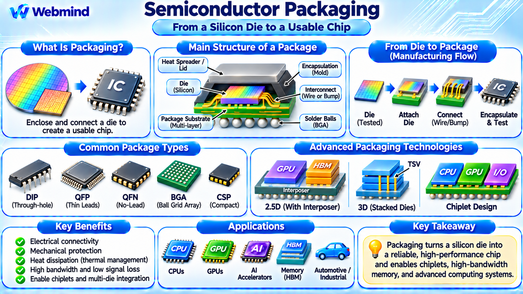
Semiconductor packaging is the process of enclosing and connecting one or more semiconductor dies to create a usable electronic component.
It provides electrical connections, mechanical protection, and thermal management for the delicate circuits manufactured on silicon wafers.
After semiconductor fabrication, individual dies are separated from the wafer and assembled into packages that can be connected to circuit boards and other electronic devices.
Packaging is essential for CPUs, GPUs, memory chips, microcontrollers, FPGAs, ASICs, and power semiconductors.
Modern semiconductor packaging has also become an important factor in computing performance.
Advanced technologies allow multiple dies, chiplets, and high-bandwidth memory devices to be integrated into a single package.
Why Do Semiconductor Chips Need Packaging?
A semiconductor die contains microscopic transistors, metal interconnections, and other electronic structures.
Although the die performs the actual computation or electrical operation, it cannot usually be installed directly onto a conventional circuit board without additional connections and protection.
Semiconductor packaging provides several important functions.
Electrical Connectivity: Connects the tiny electrical contacts on a die to larger connections that can be used by external circuits.
Mechanical Protection: Protects semiconductor structures from physical damage, contamination, and environmental exposure.
Thermal Management: Provides paths for heat to move away from the die.
Power Delivery: Supplies electrical power through conductors designed to handle the required current.
Signal Integrity: Helps maintain reliable electrical communication at high frequencies and data rates.
Advanced packages may also connect multiple dies inside one physical component.
How Does Semiconductor Packaging Work?
Semiconductor packaging begins after the main wafer fabrication process.
The wafer is electrically tested to identify dies that meet the required specifications. Individual dies are then separated through a process called dicing or singulation.
A selected die is attached to a package substrate, lead frame, or another supporting structure.
Electrical connections are created using technologies such as wire bonding, flip-chip solder bumps, or direct bonding.
The die may then be protected using molding compounds, lids, or other packaging materials.
Finally, the completed package undergoes inspection and electrical testing before shipment.
The exact process varies significantly depending on whether the product is a simple microcontroller, a high-performance CPU, a memory device, or a multi-die AI accelerator.
Main Components of a Semiconductor Package
A typical semiconductor package contains several important structures.
Semiconductor Die: The silicon circuit containing transistors and other electronic components.
Package Substrate: Provides electrical routing between the die and external contacts. Advanced substrates can contain multiple layers of fine metal wiring.
Die Attach Material: Mechanically secures the die to a supporting surface and may also provide thermal conduction.
Electrical Interconnections: Connect the die to the package through bond wires, solder bumps, copper pillars, or other technologies.
Encapsulation or Lid: Protects the die and supporting structures from physical damage and environmental conditions.
External Contacts: Provide connections between the semiconductor package and a printed circuit board.
Thermal Interface Materials: Help transfer heat from the die to a heat spreader or cooling system.
Not all packages contain every component in the same arrangement.
What Is Wire Bonding?
Wire bonding is a traditional semiconductor packaging technique used to connect the electrical pads of a die to package terminals.
Extremely thin metal wires, commonly made from gold, copper, or aluminum, form the electrical connections.
Wire bonding is widely used because it is mature, reliable, and economical for many products.
It remains common in microcontrollers, analog integrated circuits, sensors, and numerous other semiconductor devices.
However, wire bonding can become less suitable for applications requiring extremely high interconnection density or very short high-speed electrical paths.
What Is Flip-Chip Packaging?
Flip-chip packaging connects a semiconductor die to a substrate using an array of electrical contacts on the die surface.
Instead of connecting the die using wires around its edges, the die is flipped so its electrical contacts face the package substrate.
Solder bumps or other conductive structures provide the connections.
This approach supports a large number of connections distributed across the die surface.
Flip-chip technology can improve electrical performance, power delivery, and interconnection density.
It is widely used in modern CPUs, GPUs, high-performance processors, and advanced semiconductor packages.
However, flip-chip packaging requires precise assembly and careful management of mechanical stress and thermal expansion.
Common Semiconductor Package Types
Semiconductor packages are available in many physical forms.
DIP (Dual In-Line Package): Uses two rows of external pins. It is common in older electronics, educational projects, and selected components.
QFP (Quad Flat Package): Uses external leads extending from four sides of the package. It is widely used in microcontrollers and embedded electronics.
QFN (Quad Flat No-Lead): Uses contacts located underneath or near the package edges, allowing compact designs with relatively good electrical and thermal characteristics.
BGA (Ball Grid Array): Uses an array of solder balls on the bottom of the package. It supports high connection density and is common in processors, memory devices, and SoCs.
CSP (Chip Scale Package): A compact package whose dimensions are close to those of the semiconductor die.
WLCSP (Wafer-Level Chip Scale Package): Uses packaging operations performed largely at wafer level before individual devices are separated.
The package type depends on size, connection count, cost, thermal requirements, and manufacturing considerations.
What Is 2.5D Packaging?
2.5D packaging connects multiple semiconductor dies placed side by side using a high-density interposer or bridge structure.
An interposer provides electrical connections between the dies and the package substrate.
For example, an AI accelerator may contain a large compute die positioned next to several High Bandwidth Memory (HBM) stacks.
A silicon interposer or another high-density interconnect structure allows these components to exchange data through short, wide electrical connections.
This can provide much greater bandwidth than conventional board-level connections.
2.5D packaging is widely used in selected high-performance computing and AI accelerator systems.
However, it increases packaging complexity and manufacturing cost.
What Is 3D Semiconductor Packaging?
3D packaging integrates semiconductor dies vertically rather than placing all of them side by side.
Multiple dies can be stacked and electrically connected through technologies such as Through-Silicon Vias (TSVs) and hybrid bonding.
Through-Silicon Vias: Vertical conductive connections passing through a silicon die or interposer.
Hybrid Bonding: A bonding technique that combines direct dielectric bonding with fine-pitch metal connections.
Three-dimensional integration can reduce communication distances and support very high interconnection density.
For example, modern HBM devices contain vertically stacked DRAM dies connected through TSVs.
Some advanced processors also stack cache memory above compute dies to increase available cache capacity.
However, vertical stacking introduces significant challenges involving heat removal, mechanical reliability, and manufacturing yield.
Semiconductor Packaging and Chiplets
Chiplet technology divides a complex computing system into multiple semiconductor dies.
Instead of manufacturing one large monolithic processor, engineers can create separate compute, graphics, input/output, or specialized accelerator dies.
Advanced packaging connects these chiplets within a single package.
For example, a processor may combine CPU compute chiplets manufactured using an advanced process node with an input/output die manufactured using a more mature process.
This approach can improve design flexibility, manufacturing yield, and reuse of semiconductor components.
However, chiplet communication requires high-speed interconnects and careful attention to latency, bandwidth, power consumption, and signal integrity.
Technologies such as UCIe (Universal Chiplet Interconnect Express) define interfaces intended to support die-to-die communication in compatible multi-die systems.
How Does Packaging Affect Chip Performance?
Semiconductor packaging is no longer simply a protective enclosure.
Modern packages influence processor performance through electrical connectivity, memory bandwidth, and power delivery.
Interconnect Bandwidth: Short, dense connections between dies can support large amounts of data transfer.
Signal Integrity: Package wiring, impedance, and electrical losses affect high-speed communication.
Power Integrity: Package conductors must deliver stable voltage and sufficient current to increasingly powerful chips.
Thermal Performance: Heat must travel efficiently from semiconductor dies to external cooling systems.
System Integration: Multiple specialized dies can be combined to provide capabilities that would be difficult or expensive to implement monolithically.
Advanced packaging can therefore influence overall system performance as much as certain improvements in individual semiconductor components.
Thermal Management in Semiconductor Packages
Modern processors can generate substantial heat during operation.
Semiconductor packaging helps move this heat away from the active circuits.
A typical processor package may use a heat spreader and thermal interface material to transfer heat toward a cooling system.
High-performance processors may require large heatsinks, fans, liquid cooling, or other specialized cooling solutions.
Thermal challenges become more complicated in multi-die and 3D-stacked packages because some dies may be located beneath other active components.
Engineers must account for thermal resistance, material properties, power density, and mechanical reliability.
Effective thermal management is essential for maintaining processor performance and preventing overheating.
Semiconductor Packaging vs. Semiconductor Fabrication
Semiconductor fabrication and packaging are separate but closely related stages of chip production.
Fabrication: Creates transistors, electronic structures, and metal interconnections on semiconductor wafers.
Packaging: Assembles fabricated dies into usable electronic components with protection and external electrical connections.
Fabrication takes place in semiconductor manufacturing facilities using processes such as photolithography, deposition, etching, and ion implantation.
Packaging uses assembly technologies such as die attachment, wire bonding, flip-chip bonding, molding, and advanced die-to-die integration.
Both stages require precise engineering and extensive testing.
Challenges of Advanced Packaging
As semiconductor packages become more complex, manufacturers face several technical challenges.
Interconnection Density: Advanced systems require extremely fine-pitch electrical connections.
Thermal Management: Closely packed and vertically stacked dies can generate high local temperatures.
Mechanical Stress: Different materials expand and contract at different rates during temperature changes.
Manufacturing Yield: Defects in bonding or assembly can cause an otherwise functional multi-die package to fail.
Cost: Advanced substrates, interposers, bonding equipment, and assembly processes require significant investment.
Testing Complexity: Manufacturers must verify individual dies, die-to-die connections, and complete package functionality.
These challenges make packaging technology an increasingly important area of semiconductor research and development.
Where Is Advanced Packaging Used?
Advanced packaging is important in many modern electronic systems.
CPUs: Multi-die processors combine compute chiplets, cache structures, and input/output components.
GPUs: High-performance graphics processors use advanced substrates and memory integration technologies.
AI Accelerators: Often combine large compute dies with multiple HBM stacks using high-density interconnects.
Memory Devices: HBM and other stacked memory technologies depend on vertical die integration.
Mobile SoCs: Compact packaging methods help integrate processors and memory while reducing system size.
Automotive and Industrial Electronics: Specialized packages support reliability, thermal performance, and electrical requirements.
The Future of Semiconductor Packaging
As transistor scaling becomes increasingly difficult and expensive, advanced packaging offers additional ways to improve computing systems.
Chiplet architectures allow designers to combine specialized dies manufactured using different semiconductor processes.
Three-dimensional stacking can increase integration density and reduce some communication distances.
High-density interconnect technologies can also improve communication between processors and memory.
Future computing platforms are likely to depend on both advanced transistor manufacturing and increasingly sophisticated packaging technologies.
Rather than relying exclusively on smaller transistors, semiconductor designers can improve performance by optimizing how multiple dies communicate and operate together.
Conclusion
Semiconductor packaging transforms fabricated semiconductor dies into functional electronic components by providing electrical connections, mechanical protection, and thermal management.
Traditional technologies such as wire bonding, QFP, and BGA remain important, while flip-chip, 2.5D, and 3D packaging enable increasingly complex computing systems.
Advanced packaging also supports chiplet architectures, high-bandwidth memory integration, and multi-die processors.
Understanding semiconductor packaging is essential for studying silicon dies, chiplets, CPUs, GPUs, AI accelerators, semiconductor manufacturing, and modern integrated circuit design.