Introduction
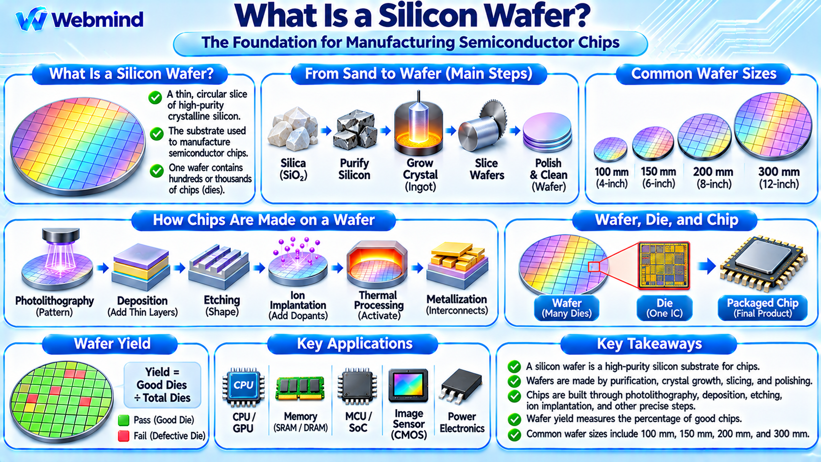
A silicon wafer is a thin, circular slice of highly purified crystalline silicon used as the foundation for manufacturing semiconductor devices.
It serves as the substrate on which transistors, diodes, sensors, memory cells, and integrated circuits are fabricated.
Silicon wafers are essential to modern semiconductor manufacturing.
They are used to produce CPUs, GPUs, microcontrollers, memory chips, FPGAs, ASICs, and many other electronic components.
A single wafer can contain hundreds or thousands of individual chips, depending on the wafer diameter and the size of each chip.
Modern semiconductor fabrication facilities, commonly called fabs, process silicon wafers through hundreds of manufacturing steps to create complex electronic circuits.
Why Is Silicon Used for Semiconductor Wafers?
Silicon is the most widely used material in semiconductor manufacturing because of its electrical properties, abundance, and mature processing technology.
Silicon is a semiconductor, meaning its electrical conductivity can be controlled by introducing impurities, applying electric fields, and modifying its physical structure.
One particularly important advantage is that silicon can form a high-quality insulating layer of silicon dioxide (SiO₂).
Silicon dioxide has historically played a critical role in manufacturing MOSFETs and other integrated circuit structures.
Silicon also provides good mechanical stability, suitable thermal properties, and compatibility with highly developed semiconductor manufacturing processes.
Although materials such as silicon carbide, gallium arsenide, and gallium nitride are used in specialized devices, silicon remains the dominant substrate for digital integrated circuits.
How Is a Silicon Wafer Made?
Manufacturing silicon wafers involves several important stages, beginning with raw materials and ending with highly polished crystalline substrates.
1. Producing High-Purity Silicon
Silicon is commonly obtained from silica, a compound found in quartz and other natural materials.
Industrial processes first convert silica into metallurgical-grade silicon.
The silicon is then purified through additional chemical processes to produce electronic-grade silicon with extremely low impurity concentrations.
High material purity is essential because unwanted impurities can affect semiconductor electrical behavior and manufacturing yield.
2. Growing a Silicon Crystal
Highly purified silicon is melted and used to grow a large single crystal called an ingot.
One common technique is the Czochralski (CZ) process.
In this method, a small seed crystal is brought into contact with molten silicon and slowly pulled upward while rotating.
Silicon atoms solidify onto the seed in an ordered crystal structure, producing a cylindrical single-crystal ingot.
Another technique, called Float-Zone (FZ) growth, can produce silicon with particularly high purity and low oxygen concentration for specialized applications.
3. Slicing the Ingot
After crystal growth, the silicon ingot is shaped and sliced into thin circular wafers using precision cutting equipment, commonly diamond-wire saws.
The wafer thickness depends on its diameter and manufacturing requirements.
For example, a typical 300 mm silicon wafer is approximately 775 micrometers thick before certain specialized thinning operations.
The slicing process must carefully control mechanical damage, surface quality, and thickness variation.
4. Grinding, Etching, and Polishing
Freshly sliced wafers contain microscopic surface damage and irregularities.
Manufacturers use grinding, chemical etching, and polishing processes to remove defects and improve surface quality.
Chemical Mechanical Polishing (CMP) combines chemical reactions with mechanical action to produce extremely flat and smooth wafer surfaces.
This level of precision is necessary because advanced semiconductor circuits contain features measured in nanometers.
5. Cleaning and Inspection
After polishing, wafers undergo extensive cleaning and inspection.
Manufacturers check surface particles, crystal defects, contamination, thickness uniformity, and other quality characteristics.
The completed wafers are then packaged and transported to semiconductor fabrication facilities.
Common Silicon Wafer Sizes
Silicon wafers are manufactured in several standard diameters.
100 mm (4-inch): Used in selected mature semiconductor processes, research, sensors, and specialized devices.
150 mm (6-inch): Common in certain analog, power semiconductor, MEMS, and industrial applications.
200 mm (8-inch): Widely used for mature-node integrated circuits, power devices, analog chips, and embedded semiconductor products.
300 mm (12-inch): The dominant wafer diameter for many advanced logic and memory manufacturing processes.
Larger wafers provide more surface area for manufacturing chips, potentially reducing production cost per chip when manufacturing yields and equipment utilization are favorable.
A 300 mm wafer has approximately 2.25 times the surface area of a 200 mm wafer.
However, larger wafers require more expensive equipment and advanced manufacturing infrastructure.
How Are Chips Manufactured on a Wafer?
Once a silicon wafer enters a semiconductor fabrication facility, it passes through many repeated processing steps.
Photolithography: Uses light-sensitive materials and optical systems to transfer circuit patterns onto the wafer.
Deposition: Adds thin layers of insulating, conducting, or semiconductor materials.
Etching: Removes selected materials to create microscopic structures.
Ion Implantation: Introduces controlled impurities into specific silicon regions to modify electrical properties.
Thermal Processing: Uses carefully controlled heating to activate dopants and modify material characteristics.
Metallization: Creates multiple layers of conductive interconnections that connect transistors and other circuit elements.
These operations are repeated to construct billions of transistors and their associated wiring.
Advanced semiconductor manufacturing may involve hundreds or thousands of individual process operations, depending on the chip design and fabrication technology.
What Is a Die?
A die is an individual integrated circuit fabricated on a semiconductor wafer.
Before separation, a wafer contains many repeated circuit patterns arranged across its surface.
For example, one 300 mm wafer may contain hundreds of relatively large processor dies or thousands of smaller integrated circuits.
The number of dies depends on the area of each design and the available wafer surface.
After fabrication, individual dies are separated through a process called dicing or singulation.
The dies are then packaged and tested according to the product requirements.
Not every fabricated die works correctly. Manufacturing defects can cause some chips to fail testing.
What Is Wafer Yield?
Wafer yield describes the proportion of manufactured dies that meet required electrical and functional specifications.
For example, if a wafer contains 500 fabricated dies and 450 pass the required tests, the simplified functional yield is 90%.
Several factors influence yield.
Defect Density: Particles and manufacturing defects can damage circuit structures.
Die Size: Larger dies generally have a greater probability of containing defects.
Process Control: Variations in fabrication conditions can affect transistor characteristics and circuit performance.
Design Complexity: Advanced designs may introduce additional manufacturing and verification challenges.
Manufacturing Maturity: Yield often improves as a fabrication process becomes more mature and better controlled.
Yield is economically important because semiconductor manufacturers invest heavily in wafers, equipment, materials, and processing time.
What Is Wafer Testing?
Before chips are separated and packaged, manufacturers commonly perform wafer-level electrical testing.
This process is often called wafer probing or wafer sort.
Automated test equipment uses probe cards to make electrical contact with test structures or pads on individual dies.
The tests help identify defective devices and measure important electrical characteristics.
Manufacturers may also classify functional dies according to performance, operating voltage, or other specifications.
After wafer testing, suitable dies proceed to packaging and additional testing.
These steps improve product reliability and reduce unnecessary packaging costs.
Silicon Wafer vs. Semiconductor Chip
A silicon wafer and a semiconductor chip are closely related but are not the same thing.
Silicon Wafer: A large circular semiconductor substrate used to manufacture many integrated circuits simultaneously.
Die: An individual circuit formed on the wafer and separated during manufacturing.
Packaged Chip: A semiconductor die, or multiple dies, assembled into a protective package with electrical connections to the outside system.
For example, a CPU begins as part of a patterned silicon wafer.
After fabrication and testing, the CPU die is separated from the wafer and assembled into a semiconductor package.
The completed processor can then be installed in a computer or integrated into another electronic device.
What Is Silicon-on-Insulator (SOI)?
Silicon-on-Insulator, or SOI, is a specialized wafer technology that places a thin silicon device layer above an insulating layer, commonly buried silicon dioxide.
This structure can reduce certain parasitic electrical effects and improve isolation between devices.
SOI technologies are used in selected RF, analog, low-power, and high-performance semiconductor applications.
One important variation is Fully Depleted Silicon-on-Insulator (FD-SOI), which supports efficient transistor operation and body-bias techniques.
SOI illustrates how wafer structure itself can influence the performance and power characteristics of semiconductor devices.
Why Are Silicon Wafers Important?
Silicon wafers are the starting point for manufacturing most modern digital integrated circuits.
Their crystal quality, purity, flatness, and mechanical properties directly influence semiconductor fabrication performance.
Wafer manufacturing also affects production cost, chip yield, and the ability to build extremely small transistor structures.
Advanced computing technologies, including artificial intelligence accelerators, high-performance processors, smartphones, and memory systems, depend on reliable wafer production.
As semiconductor manufacturing becomes more sophisticated, wafer quality and precise material engineering remain critical.
Conclusion
A silicon wafer is a thin, highly purified crystalline silicon substrate used to manufacture semiconductor devices and integrated circuits.
Its production involves silicon purification, crystal growth, precision slicing, polishing, cleaning, and inspection.
Semiconductor fabrication facilities then build transistor structures and interconnections across the wafer using processes such as photolithography, deposition, etching, and ion implantation.
After fabrication, individual dies are tested, separated, and packaged into finished semiconductor products.
Understanding silicon wafers provides an essential foundation for studying semiconductor manufacturing, transistors, CMOS technology, photolithography, CPU and GPU fabrication, and modern chip packaging.