Introduction
HBM, or High Bandwidth Memory, is an advanced DRAM technology designed to provide extremely high memory bandwidth while maintaining relatively low energy consumption per transferred bit.
It is widely used in AI accelerators, high-performance GPUs, supercomputers, and other memory-intensive computing systems.
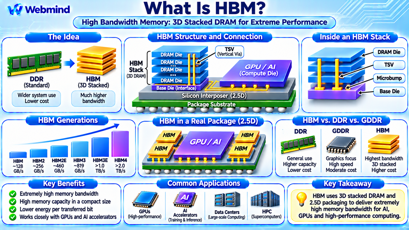
Unlike conventional DDR memory modules, HBM uses vertically stacked DRAM dies connected through thousands of high-density electrical connections.
HBM stacks are typically placed close to a processor using advanced semiconductor packaging technologies, such as 2.5D integration with a silicon interposer.
This architecture enables processors to access large amounts of data at extremely high speeds, making HBM an important technology for artificial intelligence and high-performance computing.
How Does HBM Work?
HBM uses a three-dimensional memory architecture in which multiple DRAM dies are stacked vertically.
The dies communicate through Through-Silicon Vias (TSVs), which provide electrical connections passing through the silicon layers.
A typical HBM stack contains multiple DRAM dies connected to a base die or interface layer.
The entire stack communicates with a GPU or AI accelerator through a very wide memory interface.
Instead of relying primarily on extremely high signaling frequencies, HBM achieves high bandwidth through a large number of parallel data connections.
For example, HBM2 and HBM3 generations commonly use a 1024-bit-wide interface per stack, while newer HBM technologies can provide wider interfaces.
By placing multiple HBM stacks next to a processor, a system can achieve aggregate memory bandwidth measured in terabytes per second.
Main Components of HBM
An HBM system contains several important structures.
DRAM Dies: Store information using semiconductor memory cells. Multiple dies are stacked to increase capacity.
Through-Silicon Vias (TSVs): Provide vertical electrical connections between the stacked memory dies.
Microbumps or Bonding Structures: Connect adjacent dies through small electrical contacts.
Base Die: Provides interface, control, and communication functions associated with the memory stack. Its implementation varies by HBM generation and manufacturer.
Memory Interface: Transfers data and commands between the HBM stack and the processor.
Interposer or Advanced Package Interconnect: Provides high-density electrical connections between HBM and nearby computing dies.
Memory Controller: Coordinates memory requests, addresses, timing, and data transfers.
Together, these components allow HBM to deliver high bandwidth within a compact package.
Why Does HBM Provide High Bandwidth?
Memory bandwidth describes how much data can be transferred per second.
A simplified bandwidth calculation is:
Bandwidth = Data Width × Transfer Rate ÷ 8
For example, a memory interface with 1024 data bits operating at 6.4 gigabits per second per pin provides a theoretical bandwidth of:
1024 × 6.4 Gb/s ÷ 8 = 819.2 GB/s
This illustrates how a wide interface can deliver extremely high bandwidth.
Multiple HBM stacks can operate in parallel, increasing total available bandwidth.
However, theoretical bandwidth is not the same as sustained application bandwidth.
Actual performance depends on memory access patterns, controller efficiency, system architecture, and workload characteristics.
HBM Generations: HBM, HBM2, HBM2E, HBM3, and HBM3E
HBM technology has evolved through several generations.
HBM
The original HBM generation introduced vertically stacked DRAM with a wide memory interface.
It demonstrated how three-dimensional memory integration could deliver high bandwidth using relatively low per-pin signaling rates.
HBM2
HBM2 improved data transfer rates and supported greater memory capacity.
It became important in high-performance graphics processors and scientific computing systems.
HBM2E
HBM2E extended HBM2 technology with higher transfer speeds and increased capacity.
It was used in several generations of data center accelerators and high-performance computing products.
HBM3
HBM3 introduced higher bandwidth and additional improvements in memory architecture.
It became especially important for advanced AI accelerators and large-scale machine learning systems.
HBM3E
HBM3E further increased transfer rates and capacity.
Depending on the product, HBM3E stacks can provide more than 1 TB/s of theoretical bandwidth per stack.
HBM3E has been widely adopted in high-performance AI computing hardware.
HBM4
HBM4 represents a newer generation of high-bandwidth memory technology.
Its architecture expands the interface width to 2048 bits per stack, doubling the width associated with HBM3.
HBM4 also supports increased memory capacity, greater parallelism, and higher aggregate bandwidth.
Actual capabilities depend on the implementation, operating speed, and number of stacked DRAM dies.
HBM vs. DDR Memory
HBM and DDR are both based on DRAM technology, but they are optimized for different applications.
DDR Memory: Commonly used as main system memory in desktop computers and servers. DDR modules provide relatively economical memory capacity and can be installed separately from the processor.
HBM: Uses vertically stacked DRAM dies and very wide interfaces to provide high bandwidth close to computing hardware.
DDR memory is typically connected through motherboard traces and DIMM slots.
HBM generally requires advanced packaging to connect the memory stacks to the processor.
HBM offers much greater bandwidth per stack than a conventional DDR channel, but it is more expensive and difficult to manufacture.
DDR remains more practical for many general-purpose computing systems.
HBM vs. GDDR Memory
GDDR, or Graphics Double Data Rate memory, is another high-performance DRAM technology commonly used with graphics processors.
GDDR achieves high bandwidth through high-speed signaling across memory chips positioned around the GPU on a circuit board.
HBM instead uses vertically stacked dies and a much wider interface located close to the processor.
GDDR: Generally offers a lower-cost and more conventional implementation suitable for consumer graphics cards and other bandwidth-intensive devices.
HBM: Provides very high bandwidth and can improve energy efficiency per transferred bit, but requires more complex packaging.
Both technologies are used in GPUs, depending on performance requirements, power consumption, cost, and product design.
HBM is particularly attractive for large AI accelerators and high-performance computing systems.
Why Is HBM Important for Artificial Intelligence?
Modern artificial intelligence models require enormous amounts of data to be transferred between memory and processing units.
Large language models contain billions or even trillions of parameters, depending on their architecture.
During AI inference, processors repeatedly access model weights and intermediate data.
In many workloads, memory bandwidth becomes a major performance limitation.
HBM helps address this problem by supplying data to GPUs and AI accelerators at extremely high rates.
HBM capacity is also important because model weights, activations, and the Key-Value (KV) cache used in transformer inference consume substantial memory.
For AI training, HBM supports the movement of model parameters, activations, gradients, and optimizer-related data.
However, HBM does not eliminate all performance bottlenecks. Computing throughput, communication between accelerators, software optimization, and memory capacity remain important.
HBM and 2.5D Packaging
HBM is closely associated with advanced semiconductor packaging.
A typical high-performance accelerator package contains a computing die and several HBM stacks positioned side by side.
A silicon interposer or another high-density interconnect structure connects these components.
This arrangement is commonly called 2.5D packaging.
For example, the processor can communicate with multiple HBM stacks through thousands of short electrical connections.
The short, wide interface helps support high bandwidth while limiting some of the energy costs associated with long-distance, high-speed signaling.
Technologies such as TSMC CoWoS are used to integrate computing dies and HBM in advanced semiconductor products.
Importantly, the HBM stack itself uses 3D integration, while its connection to the processor often uses 2.5D packaging.
HBM Capacity and Stack Height
HBM capacity depends on the memory density of individual DRAM dies and the number of dies in the stack.
For example, an eight-high stack containing eight DRAM dies of 24 gigabits each provides:
8 × 24 Gb = 192 Gb = 24 GB
A twelve-high stack using the same DRAM die density provides:
12 × 24 Gb = 288 Gb = 36 GB
These calculations illustrate how vertical stacking increases memory capacity.
However, taller stacks introduce additional manufacturing and thermal challenges.
The maximum supported stack height depends on the memory generation, device design, package thickness, and manufacturing technology.
Advantages of HBM
Extremely High Bandwidth: Very wide memory interfaces support massive parallel data transfers.
Energy Efficiency: Shorter interconnections and lower per-pin signaling requirements can reduce energy consumption per transferred bit.
High Integration Density: Vertically stacked DRAM provides substantial memory capacity within a compact footprint.
Advanced Processor Integration: HBM can be placed close to GPUs and AI accelerators through high-density packaging.
Scalable Bandwidth: Multiple stacks can operate in parallel to increase aggregate system bandwidth.
These characteristics make HBM valuable for advanced computing workloads.
Challenges of HBM Technology
HBM also introduces several significant engineering challenges.
Manufacturing Complexity: Stacking DRAM dies and creating TSV connections require sophisticated fabrication and assembly processes.
High Cost: Advanced packaging and complex memory manufacturing increase production expenses.
Thermal Management: Closely packed memory stacks and high-power processors create challenging cooling requirements.
Packaging Requirements: HBM generally requires specialized substrates, interposers, or other high-density interconnect technologies.
Capacity Constraints: Maximum system memory capacity depends on available stack configurations and package design.
Yield and Reliability: Defects in individual dies or vertical interconnections can affect the complete memory stack.
These factors limit HBM adoption in cost-sensitive computing products.
Where Is HBM Used?
HBM is used in several major computing applications.
AI Accelerators: Provides high-bandwidth memory for neural network training and inference.
Data Center GPUs: Supports large-scale parallel computing and memory-intensive workloads.
Supercomputers: Supplies high memory bandwidth for scientific simulations and numerical calculations.
High-Performance Computing: Accelerates applications involving large datasets and intensive mathematical operations.
Advanced Processors: Selected CPU and accelerator architectures integrate HBM to reduce memory bandwidth limitations.
Specialized ASICs: Uses HBM for networking, data processing, and other applications requiring extremely high memory throughput.
HBM is especially useful when memory bandwidth is more important than minimizing hardware cost.
The Future of HBM
The demand for high-bandwidth memory continues to grow as artificial intelligence models and computing accelerators become more complex.
Newer HBM generations are increasing interface width, memory capacity, and total bandwidth.
Manufacturers are also improving DRAM stacking, bonding technologies, base-die architectures, and packaging integration.
Future systems may combine more HBM stacks with increasingly powerful processors and specialized computing chiplets.
However, continued improvements will require solutions to thermal management, manufacturing yield, electrical reliability, and cost.
HBM development is therefore closely connected to advances in semiconductor manufacturing and packaging.
Conclusion
High Bandwidth Memory is an advanced DRAM technology that uses vertically stacked semiconductor dies and wide memory interfaces to deliver extremely high data transfer bandwidth.
Technologies such as TSVs, 3D stacking, and 2.5D packaging allow HBM to communicate efficiently with GPUs and AI accelerators.
Compared with conventional DDR and GDDR memory, HBM prioritizes bandwidth density and energy efficiency, although at higher manufacturing and packaging costs.
From HBM2 and HBM3 to HBM3E and HBM4, continued development is increasing memory capacity and bandwidth for advanced computing systems.
Understanding HBM is essential for studying GPU architecture, AI accelerators, DRAM technology, semiconductor chiplets, 2.5D packaging, and modern high-performance computing.