Introduction
Photolithography, often called lithography, is a semiconductor manufacturing process used to transfer extremely small circuit patterns onto silicon wafers.
It is one of the most important technologies in modern chip production.
Photolithography allows semiconductor manufacturers to create the microscopic structures required for transistors, logic gates, memory cells, and electrical interconnections.
Modern CPUs, GPUs, memory chips, microcontrollers, FPGAs, and ASICs all depend on lithography during manufacturing.
As semiconductor technology advances, lithography plays a critical role in increasing transistor density, improving chip performance, and enabling smaller circuit features.
How Does Photolithography Work?
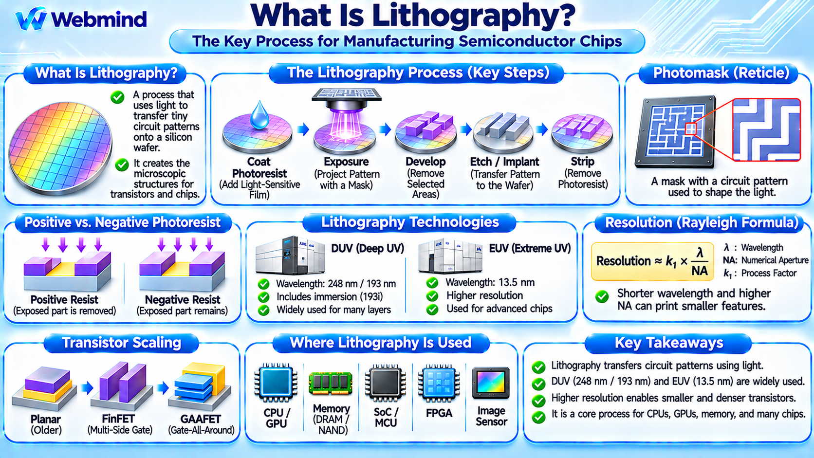
Photolithography uses light to transfer patterns from a mask onto a light-sensitive material called photoresist.
The process begins with a silicon wafer covered by a thin material layer. A coating of photoresist is applied to the wafer surface.
A lithography machine projects light through or from a patterned mask, exposing selected regions of the photoresist.
The exposure changes the chemical properties of the photoresist. During development, selected regions are removed, leaving a pattern on the wafer.
This pattern can then be used during etching, ion implantation, or other semiconductor manufacturing operations.
Photolithography does not directly create a complete transistor in one step.
Instead, many lithography cycles are combined with other fabrication processes to build complex integrated circuits.
Main Steps of Photolithography
A typical semiconductor photolithography process includes several stages.
1. Wafer Preparation
The wafer surface is cleaned and prepared to ensure that the photoresist adheres properly.
Depending on the manufacturing stage, the wafer may already contain layers of silicon dioxide, silicon nitride, metals, or other semiconductor materials.
2. Photoresist Coating
A thin layer of photoresist is applied to the wafer, commonly using a process called spin coating.
The wafer rotates at high speed to spread the liquid photoresist into a uniform film.
A baking step may then remove excess solvent and stabilize the coating.
3. Mask Alignment and Exposure
The lithography system aligns the desired circuit pattern with structures already fabricated on the wafer.
Light is used to expose selected regions of the photoresist.
Modern semiconductor fabrication commonly uses projection lithography systems that reduce and project patterns from a reticle onto the wafer.
Accurate alignment is essential because advanced semiconductor chips contain many interconnected layers.
4. Photoresist Development
After exposure and any required post-exposure baking, the wafer is treated with a chemical developer.
The developer removes selected photoresist regions, depending on the photoresist type and exposure conditions.
The remaining photoresist forms the required microscopic pattern.
5. Pattern Transfer
The patterned photoresist acts as a temporary protective layer during subsequent manufacturing operations.
For example, an etching process may remove material from exposed regions while protected regions remain intact.
Alternatively, the pattern may be used to define areas for ion implantation or other processing steps.
6. Photoresist Removal
After the required pattern-transfer operation, the remaining photoresist is removed.
The wafer can then proceed to additional deposition, etching, implantation, or lithography steps.
This sequence is repeated many times during chip manufacturing.
What Is a Photomask?
A photomask is a patterned structure used to define which regions of the wafer receive exposure.
In conventional optical lithography, the mask contains transparent and opaque or partially transmitting regions that shape the projected light.
A set of photomasks defines the different patterned layers required to manufacture an integrated circuit.
Each layer may represent transistor structures, contact openings, metal interconnections, or other circuit features.
Advanced integrated circuits require many different masks and extremely precise alignment between layers.
The cost of designing and manufacturing these masks is a significant part of advanced semiconductor development.
Positive vs. Negative Photoresist
Photoresist is a light-sensitive material whose chemical behavior changes when exposed to radiation.
Two common categories are positive and negative photoresists.
Positive Photoresist: Exposed regions become more soluble in the developer and are removed during development.
Negative Photoresist: Exposed regions become less soluble or undergo cross-linking, allowing them to remain while selected unexposed regions are removed.
Different photoresist materials are used depending on the wavelength, pattern dimensions, processing requirements, and desired manufacturing characteristics.
Advanced lithography requires carefully engineered photoresists to achieve high resolution and reliable pattern formation.
DUV Lithography: Deep Ultraviolet
DUV stands for Deep Ultraviolet.
DUV lithography uses ultraviolet light with relatively short wavelengths to print semiconductor circuit patterns.
Two important DUV wavelengths are 248 nm and 193 nm.
Modern 193 nm lithography commonly uses argon fluoride (ArF) excimer laser technology.
A major development is immersion lithography, which places a liquid, usually highly purified water, between the final projection lens and the wafer.
This increases the numerical aperture of the optical system and improves its ability to resolve small features.
DUV lithography remains widely used in semiconductor manufacturing, including many layers of advanced chips and numerous mature-node devices.
EUV Lithography: Extreme Ultraviolet
EUV stands for Extreme Ultraviolet.
EUV lithography uses light with a wavelength of approximately 13.5 nm, much shorter than conventional DUV lithography.
The shorter wavelength helps semiconductor manufacturers print smaller patterns with fewer patterning steps for certain critical layers.
EUV systems typically generate light by directing high-energy laser pulses at tiny tin droplets, creating a plasma that emits extreme ultraviolet radiation.
Because EUV light is strongly absorbed by most materials, EUV lithography uses reflective optical systems and operates in a vacuum.
Specialized multilayer mirrors guide the light through the system and project the mask pattern onto the wafer.
EUV lithography is used for selected critical layers in advanced semiconductor manufacturing.
However, DUV and EUV processes continue to coexist because not every layer requires EUV resolution.
What Is High-NA EUV Lithography?
Numerical Aperture (NA) is an optical parameter related to the ability of a lithography system to resolve fine features.
Conventional EUV lithography systems use a numerical aperture of approximately 0.33.
High-NA EUV systems increase this value to approximately 0.55.
A higher numerical aperture can improve achievable resolution and help manufacturers produce smaller circuit features.
However, High-NA EUV introduces additional challenges involving optical design, depth of focus, mask technology, resist performance, and manufacturing cost.
High-NA EUV represents an important development in advanced semiconductor lithography, particularly for future generations of highly scaled integrated circuits.
What Determines Lithography Resolution?
The resolution of an optical lithography system depends on several factors, including wavelength, numerical aperture, and process technology.
A simplified relationship is expressed by the Rayleigh resolution equation:
Resolution ≈ k₁ × λ / NA
Where:
λ (Lambda): The wavelength of the light used for exposure.
NA: The numerical aperture of the optical system.
k₁: A factor representing process and imaging conditions.
Reducing the wavelength or increasing numerical aperture can improve the ability to print smaller features.
However, actual semiconductor patterning also depends on photoresist chemistry, optical corrections, process variability, and pattern design.
Modern lithography uses advanced computational techniques to optimize mask patterns and improve printed feature accuracy.
What Is Multiple Patterning?
Multiple patterning is a technique used when a single lithography exposure cannot produce the required pattern density.
Instead of creating all features in one exposure, manufacturers divide the pattern into multiple processing steps.
These may involve additional exposures, etching operations, or self-aligned patterning techniques.
Multiple patterning has been widely used with DUV lithography to manufacture advanced semiconductor features.
Although it enables smaller structures, it also increases manufacturing complexity, processing time, and cost.
EUV lithography can reduce the number of patterning steps required for certain critical layers, but multiple patterning may still be necessary for some advanced designs.
Why Is Lithography Important for Transistor Scaling?
Lithography strongly influences how closely transistors and electrical interconnections can be placed on a semiconductor die.
Smaller and more densely packed circuit features allow manufacturers to integrate additional functionality within a given silicon area.
This can improve computing capability and enable more sophisticated processor architectures.
However, reducing transistor dimensions also introduces challenges involving leakage current, power density, interconnect resistance, and manufacturing variability.
Advanced structures such as FinFETs and Gate-All-Around FETs (GAAFETs) help address some transistor-scaling limitations.
Lithography works together with materials engineering, transistor design, etching, deposition, and advanced packaging to support continued semiconductor development.
It is important to understand that process-node names such as 3 nm and 2 nm do not directly represent the wavelength of lithography light or the exact physical size of every transistor feature.
Who Makes Semiconductor Lithography Equipment?
Semiconductor lithography requires highly specialized equipment and advanced optical engineering.
ASML: Develops advanced lithography systems, including EUV and High-NA EUV equipment, as well as DUV systems.
Nikon: Produces lithography equipment used in various semiconductor manufacturing applications.
Canon: Develops semiconductor lithography equipment, including systems for selected mature-node and specialized manufacturing processes.
Lithography equipment is used by semiconductor manufacturers and foundries to produce integrated circuits.
The complete semiconductor manufacturing process also depends on suppliers of photoresists, masks, optical components, metrology equipment, and other specialized technologies.
Applications of Photolithography
Photolithography is essential in many semiconductor manufacturing applications.
CPUs and GPUs: Defines transistor structures and interconnections used in high-performance computing processors.
Memory Chips: Supports the manufacturing of DRAM and NAND Flash structures.
Microcontrollers and SoCs: Creates integrated digital and mixed-signal circuits.
FPGAs and ASICs: Produces programmable logic devices and application-specific integrated circuits.
Image Sensors: Helps define pixel arrays, transistors, and supporting electronic circuits.
MEMS Devices: Is used to create microscopic mechanical and electronic structures for sensors and actuators.
Power Semiconductors: Supports the fabrication of MOSFETs and other power-control devices.
Challenges of Modern Lithography
As semiconductor features become smaller, lithography becomes increasingly difficult and expensive.
Resolution Limits: Optical systems must resolve extremely small circuit patterns.
Overlay Accuracy: Different circuit layers must align with nanometer-scale precision.
Defect Control: Tiny particles or patterning defects can cause circuit failures.
Photoresist Performance: Materials must balance resolution, sensitivity, and pattern quality.
Equipment Complexity: Advanced EUV systems require specialized optics, light sources, vacuum systems, and precise mechanical control.
Manufacturing Cost: Advanced lithography equipment, masks, and processing steps require substantial investment.
These challenges make lithography one of the most technically demanding areas of semiconductor manufacturing.
Conclusion
Photolithography is a semiconductor manufacturing process that uses light-sensitive materials and precisely controlled exposure systems to transfer microscopic circuit patterns onto silicon wafers.
DUV and EUV technologies enable the fabrication of advanced integrated circuits, while High-NA EUV extends the possibilities for printing increasingly fine structures.
Lithography works together with deposition, etching, ion implantation, and other processes to manufacture transistors and the interconnections that form modern chips.
Understanding photolithography is an important foundation for studying silicon wafers, semiconductor fabrication, CMOS technology, transistor scaling, CPUs, GPUs, memory chips, and advanced semiconductor manufacturing.