Introduction
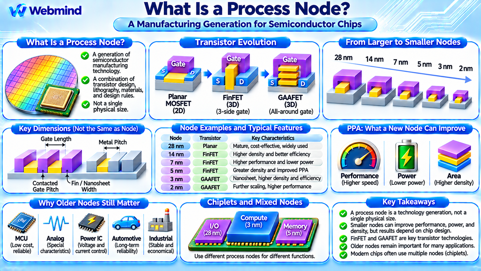
A semiconductor process node, also called a technology node or manufacturing node, refers to a generation of semiconductor manufacturing technology used to produce integrated circuits.
Process nodes are commonly identified by names such as 28nm, 14nm, 7nm, 5nm, 3nm, and 2nm.
These names are widely used to describe the evolution of semiconductor manufacturing and are important in the development of CPUs, GPUs, smartphone processors, and artificial intelligence accelerators.
Historically, process-node names were closely associated with physical transistor dimensions.
However, modern node names no longer correspond directly to a single measurable feature, such as transistor gate length.
Instead, a process node represents a combination of transistor architecture, manufacturing techniques, circuit density, performance, power efficiency, and interconnect technology.
What Does the Nanometer Number Mean?
A nanometer (nm) is one billionth of a meter.
In earlier semiconductor generations, process-node names were often associated with dimensions such as transistor gate length or metal interconnect pitch.
As semiconductor manufacturing advanced, the relationship between node names and physical dimensions became less direct.
For example, a chip manufactured using a 3nm process does not contain transistors whose every important dimension measures exactly three nanometers.
The term 3nm is primarily a manufacturing technology designation.
Similarly, a 2nm process is not necessarily 50 percent smaller than a 4nm process in every physical dimension.
Different semiconductor manufacturers use their own naming conventions, making direct comparisons between process nodes difficult.
How Does a Process Node Work?
A semiconductor process node defines a collection of manufacturing capabilities and design rules used to fabricate integrated circuits.
These include transistor structures, lithography requirements, material choices, metal interconnect dimensions, electrical characteristics, and standard-cell design rules.
When engineers design a chip, they use a Process Design Kit (PDK) provided by the semiconductor foundry.
The PDK contains transistor models, layout rules, electrical parameters, and other information required to create circuits compatible with the selected process.
Electronic Design Automation (EDA) tools use this information during circuit design, simulation, synthesis, placement, routing, and physical verification.
After the design is completed, the foundry manufactures the chip using the corresponding semiconductor process.
How Have Process Nodes Evolved?
Semiconductor manufacturing has progressed through many generations.
90nm and 65nm: Supported continued scaling of planar CMOS transistors and were widely used in earlier generations of processors and embedded devices.
45nm and 32nm: Introduced important improvements in transistor materials and manufacturing techniques, including wider adoption of high-k metal-gate technology.
22nm and 14nm: Marked an important transition toward three-dimensional FinFET transistor structures in advanced logic manufacturing.
10nm and 7nm: Increased transistor density and manufacturing complexity, with advanced patterning techniques becoming increasingly important.
5nm and 3nm: Extended transistor scaling through advanced lithography, improved transistor structures, and sophisticated process integration.
2nm-Class Technologies: Represent another generation of advanced manufacturing, with nanosheet Gate-All-Around Field-Effect Transistors (GAAFETs) becoming important in several leading-edge processes.
These names describe broad technology generations rather than identical manufacturing methods across different companies.
Process Node vs. Transistor Size
A process node should not be confused with the actual dimensions of a transistor.
Modern transistors contain several important geometric features.
Gate Length: The physical length of the gate region that controls the semiconductor channel.
Contacted Gate Pitch: The spacing between neighboring gate structures, including their associated contacts.
Metal Pitch: The spacing between adjacent metal interconnection lines.
Fin Width or Nanosheet Dimensions: Physical dimensions of the conducting channel in advanced transistor structures.
Standard-Cell Height: A layout parameter that influences the density of digital logic circuits.
These dimensions collectively affect transistor density, performance, and manufacturing complexity.
A process-node name alone does not provide enough information to determine these characteristics.
Process Nodes and Transistor Architecture
Semiconductor scaling has required major changes in transistor structure.
Planar MOSFET
Traditional planar MOSFETs use a relatively flat semiconductor channel controlled primarily by a gate positioned above it.
Planar transistor technology dominated semiconductor manufacturing for decades and remains widely used in mature-node products.
FinFET
A FinFET uses a vertical fin-shaped channel.
The gate controls multiple sides of the fin, providing stronger electrostatic control and reducing certain short-channel effects.
FinFETs became a major technology for advanced logic manufacturing beginning in the 2010s.
GAAFET
A Gate-All-Around Field-Effect Transistor surrounds the semiconductor channel with the gate.
Modern implementations commonly use stacked nanosheets.
This architecture provides improved channel control and additional flexibility for advanced transistor scaling.
However, transistor architecture is not determined solely by the node name. Different manufacturers may use different transistor structures at similarly named process nodes.
How Does Lithography Affect Process Nodes?
Photolithography is one of the most important technologies used in semiconductor manufacturing.
It transfers microscopic circuit patterns onto silicon wafers using light-sensitive materials and precision optical systems.
Deep Ultraviolet (DUV) lithography has been widely used across many semiconductor generations.
Extreme Ultraviolet (EUV) lithography uses light with a wavelength of approximately 13.5nm, helping manufacturers print smaller features with fewer patterning steps for certain critical layers.
Advanced processes may combine EUV and DUV lithography because different chip layers have different resolution requirements.
High-NA EUV technology further increases the numerical aperture of lithography equipment, offering additional resolution improvements.
However, smaller process nodes also require advances in etching, deposition, materials engineering, and manufacturing control.
Lithography alone does not determine transistor density or chip performance.
Does a Smaller Process Node Mean a Faster CPU?
A smaller process node can provide opportunities to improve processor performance, but it does not automatically make a chip faster.
Modern semiconductor processes are often optimized around three major characteristics:
Performance: Higher switching speeds or improved electrical characteristics may allow circuits to operate faster.
Power: Improved transistor designs can reduce energy consumption for certain operating conditions.
Area: Higher transistor density can allow more circuitry to fit within a given silicon area.
These characteristics are commonly summarized as PPA: Power, Performance, and Area.
However, improvements involve trade-offs.
For example, a process optimized for maximum performance may consume more power than a lower-frequency implementation.
Actual CPU performance also depends on architecture, clock frequency, cache design, memory bandwidth, thermal limits, and software workloads.
A well-designed processor using an older process can outperform a less efficient design manufactured using a newer process.
What Is Transistor Density?
Transistor density describes how many transistors can be integrated into a given silicon area.
It is often expressed as millions of transistors per square millimeter.
Smaller process nodes generally aim to increase transistor density, but the improvement varies according to the transistor type and circuit being manufactured.
Logic circuits, SRAM memory cells, analog components, and input/output structures do not necessarily scale at the same rate.
For example, an advanced process may significantly improve logic density while providing a smaller improvement in SRAM cell area.
This is one reason transistor density cannot be determined reliably from node names alone.
Comparisons between manufacturers must consider actual design rules, standard-cell libraries, circuit structures, and measurement methods.
Why Are Advanced Process Nodes Expensive?
Developing and manufacturing advanced semiconductor processes requires enormous investment.
Lithography Equipment: Advanced EUV systems and related equipment are extremely expensive.
Manufacturing Complexity: Smaller circuit features require tighter process control and more sophisticated fabrication steps.
Mask Costs: Advanced chips may require complex photomasks and extensive design verification.
Research and Development: New transistor architectures, materials, and process technologies require years of engineering effort.
Yield Management: Manufacturing defects and process variations can reduce the number of functional chips produced from each wafer.
Design Costs: Advanced nodes often require more complex EDA tools, verification, and physical design optimization.
These factors explain why not every semiconductor product uses the newest manufacturing node.
Why Are Older Process Nodes Still Important?
Many electronic products do not require the highest possible transistor density.
Mature manufacturing nodes such as 180nm, 90nm, 65nm, 40nm, and 28nm remain important for numerous applications.
Microcontrollers: Often prioritize low cost, reliability, integrated peripherals, and long product lifetimes.
Analog Chips: May require specialized transistor characteristics that are not available or economical on the newest logic nodes.
Power Management ICs: Focus on voltage handling, current control, efficiency, and manufacturing cost.
Automotive Electronics: Frequently emphasize reliability, qualification, and long-term supply availability.
Industrial Systems: Often use mature semiconductor technologies with well-established manufacturing processes.
Older process nodes can therefore remain economically valuable for many years.
Process Nodes and Chiplets
As advanced semiconductor manufacturing becomes more expensive, chip designers increasingly use chiplet-based architectures.
Instead of manufacturing every function on one large die using a single process node, engineers can divide a system into multiple dies.
For example, CPU compute chiplets may use an advanced manufacturing process, while an input/output die uses a more mature and economical process.
These dies are connected through advanced semiconductor packaging.
This approach allows manufacturers to select appropriate technologies for different functions.
However, chiplets introduce additional challenges involving interconnect bandwidth, latency, power delivery, thermal management, and packaging cost.
How Should Process Nodes Be Compared?
Comparing process nodes requires more than looking at nanometer labels.
Important factors include transistor density, power efficiency, switching performance, SRAM scaling, interconnect characteristics, manufacturing yield, and production cost.
For example, two foundries may both offer a process described as 3nm, but the underlying transistor structures, design rules, and achievable circuit characteristics may differ.
Even within one manufacturer, different process variants may be optimized for high performance, low power, or other requirements.
Therefore, node names are most useful as indicators of technology generations rather than precise measures of chip performance.
Conclusion
A semiconductor process node represents a generation of integrated circuit manufacturing technology, including transistor architecture, lithography, materials, design rules, and electrical characteristics.
Names such as 7nm, 5nm, 3nm, and 2nm no longer correspond directly to a single physical transistor dimension.
Smaller nodes can enable improvements in transistor density, performance, and energy efficiency, but actual results depend on chip design and manufacturing technology.
At the same time, mature process nodes remain essential for microcontrollers, analog circuits, power electronics, and industrial devices.
Understanding semiconductor process nodes provides an important foundation for studying transistor scaling, FinFETs, GAAFETs, photolithography, silicon wafers, chiplets, and modern semiconductor manufacturing.