Introduction
A chiplet is a small semiconductor die designed to work together with other dies inside a single semiconductor package.
Instead of manufacturing an entire processor as one large piece of silicon, chiplet technology divides the system into smaller functional components.
These components can include CPU cores, graphics processors, memory controllers, input/output interfaces, and specialized hardware accelerators.
Chiplets are becoming increasingly important in modern CPUs, GPUs, AI accelerators, and high-performance computing systems.
They provide an alternative to traditional monolithic chip designs, offering greater flexibility in semiconductor manufacturing and system integration.
By combining multiple dies within one package, chip designers can build complex computing systems without placing every function on the same silicon die.
How Does Chiplet Technology Work?
A chiplet-based processor divides its major functions into separate semiconductor dies.
For example, a processor may contain multiple CPU compute chiplets and a separate input/output die.
The compute chiplets perform arithmetic operations, execute instructions, and process data.
The input/output die may contain memory controllers, PCI Express interfaces, and other communication hardware.
These components communicate through high-speed interconnections inside the semiconductor package.
Although the system contains multiple dies, it can operate as a unified processor from the perspective of software.
Chiplet technology therefore changes how a processor is physically constructed without necessarily changing its Instruction Set Architecture (ISA).
Monolithic Chip vs. Chiplet Design
Traditional processors are often manufactured as monolithic integrated circuits.
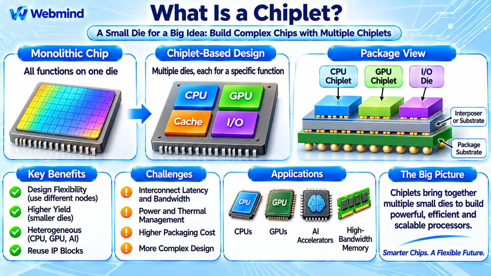
A monolithic chip integrates its processing units, memory interfaces, and other major functions onto a single semiconductor die.
A chiplet-based design separates selected functions into multiple dies.
Monolithic Design: All major components are fabricated together on one die. This can simplify internal communication and avoid some inter-die connection overhead.
Chiplet Design: Different functions are manufactured on separate dies and connected through advanced packaging.
Chiplet architectures can provide greater manufacturing flexibility and potentially improve production economics.
However, communication between chiplets introduces additional challenges involving latency, bandwidth, power consumption, and packaging complexity.
Neither design approach is automatically superior for every application.
Main Components of a Chiplet-Based Processor
A chiplet-based system may contain several different types of dies.
Compute Chiplets: Contain CPU cores, caches, and other processing resources.
I/O Die: Provides memory controllers, PCIe interfaces, and communication functions.
GPU Chiplets: Implement selected graphics or parallel computing functions.
AI Accelerator Chiplets: Contain specialized hardware for matrix multiplication and neural network operations.
Memory Dies: Provide high-bandwidth memory or other specialized storage resources.
Interconnect Structures: Transfer signals and data between chiplets through package-level connections.
Package Substrate or Interposer: Provides mechanical support and electrical connections between dies and external devices.
The exact configuration depends on the processor architecture and intended workload.
How Do Chiplets Communicate?
Chiplets must exchange data efficiently to function as one computing system.
Modern multi-die processors use high-speed die-to-die interconnects that provide communication between neighboring dies.
These connections may carry data, control signals, memory transactions, or coherence information.
Some chiplet-based systems use proprietary interconnect technologies, while others adopt standardized interfaces.
One important industry standard is UCIe (Universal Chiplet Interconnect Express).
UCIe defines specifications for die-to-die communication, helping support interoperability between compatible chiplet designs.
However, UCIe compatibility does not automatically mean that any two chiplets from different manufacturers can be combined without additional integration and validation.
Chiplet communication must also address signaling, power delivery, clocking, error handling, and thermal requirements.
What Is Advanced Semiconductor Packaging?
Advanced packaging technologies allow multiple semiconductor dies to be connected within a single package.
Several important approaches are used.
2D Packaging
Multiple dies are mounted on a common package substrate and connected through electrical routing structures.
This approach can be relatively straightforward but may limit achievable interconnect density.
2.5D Packaging
Multiple dies are placed side by side and connected through a high-density interposer or bridge structure.
This approach can provide high-bandwidth communication between processors and memory devices.
It is widely used in certain high-performance computing and AI accelerator packages.
3D Packaging
Semiconductor dies are stacked vertically and connected through technologies such as Through-Silicon Vias (TSVs), hybrid bonding, or other advanced interconnect methods.
Three-dimensional integration can reduce communication distances and increase packaging density.
However, stacked dies introduce significant thermal and manufacturing challenges.
Why Can Chiplets Improve Manufacturing Yield?
Semiconductor manufacturing defects can cause individual dies to fail testing.
As die area increases, the probability of encountering a manufacturing defect generally increases.
A large monolithic processor may therefore have a lower functional yield than several smaller dies manufactured using similar technology.
Chiplet designs allow manufacturers to fabricate and test smaller dies individually.
Functional dies can then be selected for packaging, while defective dies can be rejected before assembly.
This approach can improve the effective use of semiconductor wafers.
However, overall product yield also depends on packaging quality, interconnect reliability, die testing, and assembly processes.
Chiplets do not automatically reduce total manufacturing cost in every situation.
Chiplets and Different Process Nodes
One major advantage of chiplet technology is the ability to combine dies manufactured using different semiconductor process nodes.
For example, CPU compute chiplets may use an advanced process optimized for transistor density and performance.
A separate I/O die may use a more mature process that is suitable for memory controllers, analog interfaces, and other supporting functions.
This approach is commonly called heterogeneous integration.
It allows designers to select manufacturing technologies according to the needs of individual components.
Advanced process nodes are expensive, so using them only where necessary can improve overall manufacturing economics.
However, mixing process nodes requires careful attention to electrical interfaces, packaging design, power delivery, and thermal behavior.
Chiplets in Modern CPUs and GPUs
Chiplet technology is already used in commercial processors.
AMD Ryzen and EPYC: Many AMD processors use separate compute dies and I/O dies connected through high-speed internal interconnects.
Intel Processors: Intel uses advanced multi-die and tiled packaging approaches in selected processor families, combining different functional blocks within one package.
Advanced GPUs: Some GPU architectures use multiple semiconductor dies or chiplet-like structures for graphics processing, memory interfaces, or supporting functions.
AI Accelerators: High-performance accelerators may combine compute dies with high-bandwidth memory through advanced packaging.
These architectures demonstrate that modern processors increasingly depend on system-level integration rather than simply manufacturing larger monolithic silicon dies.
Chiplets vs. SoC: What Is the Difference?
A System-on-Chip (SoC) integrates multiple computing functions into a highly integrated system, traditionally on one semiconductor die.
A chiplet describes an individual die designed to operate with other dies in a larger package.
The two concepts are related but not identical.
A monolithic SoC may integrate CPU cores, GPUs, memory controllers, and communication interfaces onto one die.
A multi-die system may provide similar integrated functionality using several chiplets inside one package.
Chiplets therefore describe a physical integration strategy, while SoC describes a high level of system functionality and integration.
The terms can overlap in advanced semiconductor products.
Advantages of Chiplet Technology
Improved Manufacturing Flexibility: Different functions can be manufactured separately using suitable process technologies.
Potential Yield Improvements: Smaller dies can reduce the impact of manufacturing defects.
Scalability: Designers can combine multiple compute chiplets to create processors with different performance levels.
Design Reuse: Existing chiplet designs may be reused across multiple products.
Heterogeneous Integration: CPU, GPU, AI, memory, and specialized functions can be combined within one package.
Advanced Packaging Options: High-density interconnections enable sophisticated multi-die architectures.
These advantages make chiplets attractive for complex computing systems.
Challenges of Chiplet Technology
Despite their benefits, chiplets introduce new engineering problems.
Interconnect Latency: Communication between dies may require more time than communication within one monolithic die.
Bandwidth Requirements: High-performance systems need very fast connections between chiplets.
Power Consumption: Die-to-die communication consumes electrical energy.
Thermal Management: Multiple dies within one package can create difficult cooling conditions.
Packaging Cost: Advanced substrates, interposers, bonding technologies, and assembly processes can be expensive.
Testing and Reliability: Manufacturers must verify individual dies, package connections, and complete system operation.
Design Complexity: Engineers must coordinate clock domains, memory coherence, interconnect protocols, and power management across multiple dies.
These factors influence whether a chiplet-based architecture is practical for a particular product.
Chiplets and the Future of Semiconductor Design
Chiplet technology is becoming increasingly important as advanced semiconductor manufacturing grows more complex and expensive.
Instead of relying entirely on smaller transistors, chip designers can improve system capabilities by combining specialized dies.
For example, future computing packages may integrate general-purpose CPU chiplets, AI accelerators, high-bandwidth memory, and communication interfaces.
Open die-to-die standards such as UCIe may help expand the ecosystem for reusable chiplet components.
At the same time, advanced packaging technologies are expected to play a larger role in determining processor performance, energy efficiency, and manufacturing cost.
Chiplets complement transistor scaling rather than replace it.
Conclusion
A chiplet is a semiconductor die designed to operate together with other dies inside a single package.
By dividing complex processors into smaller functional components, chiplet technology provides greater design flexibility and enables the integration of different manufacturing processes.
Modern CPUs, GPUs, and AI accelerators increasingly use multi-die architectures supported by advanced interconnect and packaging technologies.
Although chiplets introduce challenges involving communication, power, cooling, and manufacturing complexity, they offer important opportunities for building scalable computing systems.
Understanding chiplets is essential for studying semiconductor dies, process nodes, advanced packaging, SoCs, CPU and GPU architectures, and the future of integrated circuit design.