Introduction
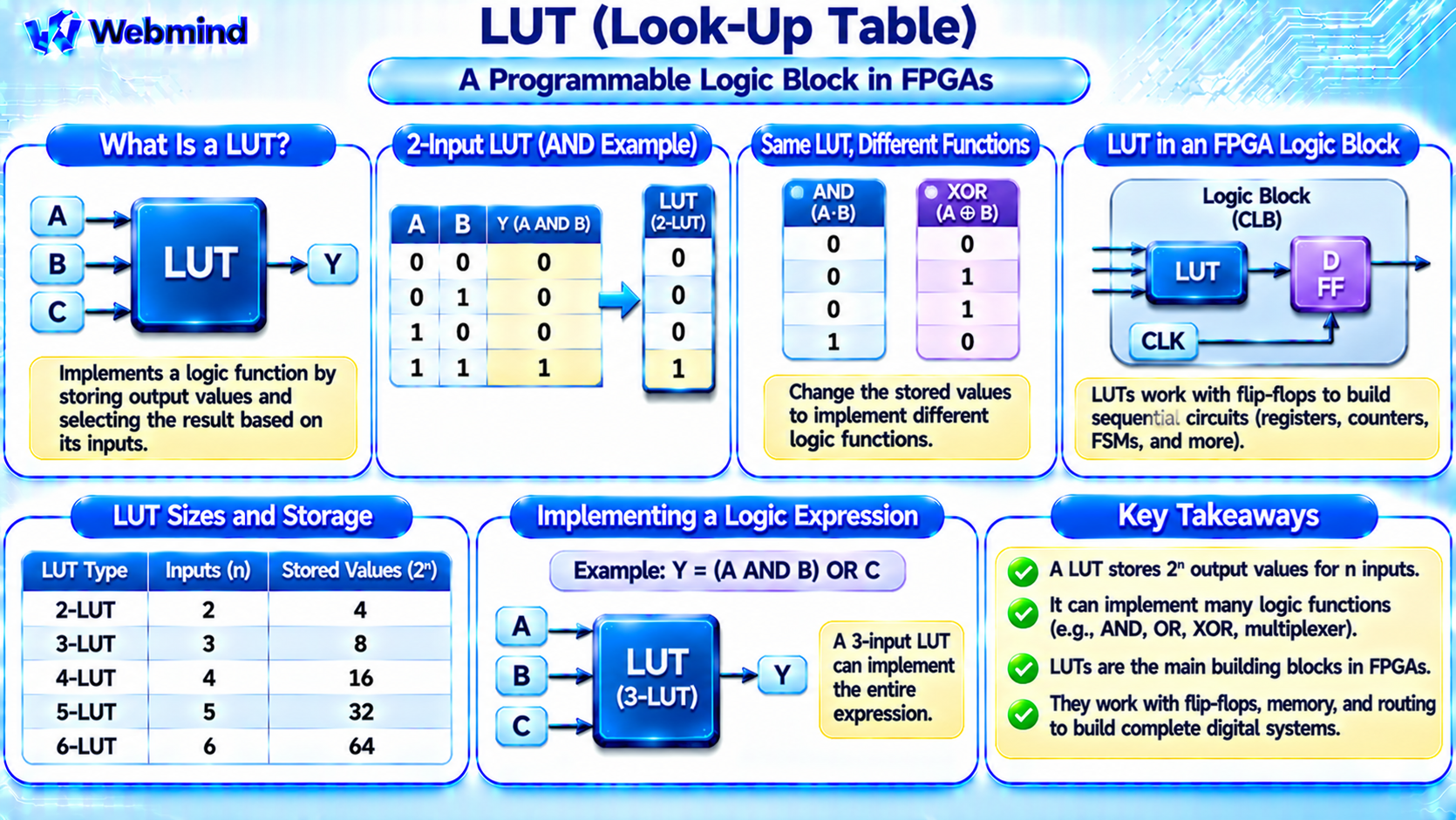
A LUT, or Look-Up Table, is a digital logic structure that stores predefined output values and selects the appropriate result based on its input signals.
LUTs are fundamental building blocks of Field-Programmable Gate Arrays (FPGAs), allowing programmable hardware to implement different Boolean logic functions.
Unlike a conventional logic gate that performs one fixed operation, such as AND or OR, a LUT can be configured to perform many different logic functions without changing the physical circuitry.
For example, the same two-input LUT can implement an AND gate, OR gate, XOR gate, or NAND gate simply by changing its stored truth-table values.
Understanding LUTs is essential for learning FPGA architecture, digital logic, Boolean algebra, and Verilog hardware design.
How Does a LUT Work?
A LUT implements a Boolean function by storing its possible output values.
Consider a logic function with two binary inputs, A and B.
Because each input can be either 0 or 1, there are four possible input combinations: 00, 01, 10, and 11.
A two-input LUT stores four output bits, one for each combination.
When the input signals change, the LUT selects the corresponding stored bit and presents it at its output.
The inputs effectively act as selection signals, similar to the select inputs of a multiplexer.
The stored values determine the Boolean function implemented by the LUT.
This makes the LUT a flexible and reusable hardware resource.
What Is a 2-Input LUT?
A two-input LUT, commonly called a 2-LUT, has two logical inputs and can implement any Boolean function of those inputs with one output.
For example, consider an AND function.
Its truth-table outputs are:
A = 0, B = 0 → Y = 0
A = 0, B = 1 → Y = 0
A = 1, B = 0 → Y = 0
A = 1, B = 1 → Y = 1
The LUT stores the corresponding output pattern:
0, 0, 0, 1
When A and B are both 1, the LUT selects the stored value 1. For the other input combinations, it selects 0.
Now consider an XOR function.
Its output pattern is:
0, 1, 1, 0
Loading this pattern into the same LUT changes its behavior from AND to XOR.
No physical rewiring is required.
How Many Values Does a LUT Store?
A LUT with n binary inputs must represent 2ⁿ possible input combinations.
For a single-output LUT, this requires 2ⁿ stored output bits.
Common examples include:
2-LUT: 2 inputs and 4 stored output bits.
3-LUT: 3 inputs and 8 stored output bits.
4-LUT: 4 inputs and 16 stored output bits.
5-LUT: 5 inputs and 32 stored output bits.
6-LUT: 6 inputs and 64 stored output bits.
For example, a 4-LUT can implement any Boolean function with up to four inputs and one output.
A 6-LUT can implement any single-output Boolean function with up to six inputs.
However, actual FPGA devices may support additional LUT configurations, shared outputs, and specialized logic structures.
How Is a LUT Built Inside an FPGA?
A conventional SRAM-based FPGA LUT can be understood as a collection of configuration memory bits connected to a multiplexer selection network.
The configuration memory stores the truth-table outputs.
The input signals control the selection network, which chooses one stored value.
For example, a 4-LUT contains sixteen possible truth-table output values.
Its four input signals select one of these sixteen values.
Modern FPGA implementations may use optimized transistor-level selection circuits rather than a simple collection of separate multiplexers.
Some FPGA families also use different configuration technologies.
The fundamental principle remains the same: the LUT selects a predefined output based on the current input combination.
LUT vs. Logic Gate: What Is the Difference?
A conventional logic gate implements a specific Boolean operation.
For example, an AND gate produces 1 only when all its inputs are 1.
An OR gate produces 1 when at least one input is 1.
A LUT is more flexible because its Boolean function is determined by stored configuration values.
A two-input LUT can be configured as AND, OR, XOR, NAND, NOR, XNOR, or another two-input Boolean function.
This flexibility is one of the reasons FPGAs can implement many different digital circuits using the same physical hardware resources.
However, a LUT is not necessarily faster or smaller than a dedicated logic gate.
The advantage of a LUT is programmability rather than always achieving the lowest transistor count or propagation delay.
LUT vs. Truth Table
A truth table is a mathematical representation of a Boolean function.
A LUT is a physical hardware structure that can store and implement that function.
For example, a two-input XOR truth table specifies:
00 → 0
01 → 1
10 → 1
11 → 0
A two-input LUT can store these four output values.
When the inputs are applied, the LUT produces the corresponding output.
The truth table describes what the function does, while the LUT provides a hardware mechanism for implementing it.
This relationship connects Boolean algebra directly to programmable digital hardware.
How Does a LUT Implement Complex Logic?
A LUT can implement more than individual AND or OR gates.
Consider the Boolean expression:
Y = (A AND B) OR C
This function has three independent inputs: A, B, and C.
A 3-LUT contains eight possible output values, corresponding to the eight input combinations.
The required output values can be stored directly in the LUT.
As a result, the complete Boolean function can be implemented using one 3-LUT rather than separate AND and OR gates, assuming the target FPGA architecture supports the required LUT configuration.
This demonstrates how LUTs can combine multiple logical operations into a single programmable resource.
How Are Multiple LUTs Connected?
A complex digital circuit may contain Boolean functions with more inputs than one LUT can support.
For example, a function requiring eight independent inputs cannot always be implemented in a single 6-LUT.
FPGA synthesis tools can divide the function into smaller logic networks and map those networks onto multiple LUTs.
The LUTs are connected using programmable routing resources.
A signal produced by one LUT may become an input to another LUT.
This creates a network of configurable logic capable of implementing complex circuits.
However, each additional LUT and routing connection may introduce propagation delay and consume hardware resources.
EDA tools optimize the implementation to balance timing, area, and power requirements.
LUTs and Flip-Flops in FPGAs
LUTs and flip-flops perform different functions.
LUT: Implements combinational logic. Its output depends on the current input values and the stored configuration.
Flip-Flop: Stores one bit of information and typically updates its state at a clock edge.
Modern FPGAs commonly place LUTs and flip-flops within configurable logic blocks or related programmable structures.
For example, an FPGA counter uses logic to calculate the next count value and registers to store the current count.
LUTs can implement the next-state logic, while flip-flops store the state.
Together, these resources support sequential circuits such as counters, registers, state machines, and controllers.
LUTs in FPGA Logic Blocks
Modern FPGAs organize programmable logic into larger structures containing LUTs, registers, routing connections, and sometimes additional arithmetic resources.
Different FPGA manufacturers use different architectural terminology.
AMD FPGA architectures include configurable logic blocks and related logic resources.
Intel FPGA architectures use structures such as Adaptive Logic Modules (ALMs), which provide configurable logic and register resources.
The exact number of LUT inputs, available outputs, and logic-sharing capabilities varies by device family.
For example, some FPGA architectures allow a larger LUT to be divided into smaller logic functions under specific input-sharing conditions.
Understanding these architectural details helps FPGA designers use hardware resources efficiently.
How Does Verilog Become LUT Hardware?
FPGA developers normally do not need to manually enter every LUT truth table.
Instead, they describe the required circuit behavior using Verilog, SystemVerilog, or VHDL.
For example, the Verilog statement:
assign y = (a & b) | c;
describes a Boolean function containing AND and OR operations.
The synthesis tool analyzes the expression and determines how it can be mapped onto the target FPGA’s logic resources.
For a compatible FPGA architecture, the tool may implement the entire function using one LUT.
The implementation tools then place the LUT into an available logic block and connect it using programmable routing.
Finally, the FPGA development software generates a configuration bitstream.
The bitstream determines the LUT configuration, routing connections, and other programmable hardware settings.
What Is LUT Utilization?
LUT utilization describes how many LUT resources a design uses within an FPGA.
For example, suppose an FPGA provides 20,000 available LUT resources and a design uses 5,000.
The simplified LUT utilization is:
5,000 ÷ 20,000 × 100% = 25%
However, FPGA resource reports may use different definitions depending on the device architecture and how LUTs are shared or combined.
Higher LUT utilization means fewer remaining resources are available for additional logic.
Very high utilization can also make placement and routing more difficult.
FPGA designers therefore monitor LUT utilization, register usage, memory blocks, DSP resources, and timing performance.
Does More LUTs Mean Better FPGA Performance?
A larger number of LUTs generally provides more capacity for programmable logic, but it does not automatically mean higher performance.
FPGA performance depends on several factors.
LUT Architecture: The number of inputs and available configurations influence how efficiently logic can be mapped.
Routing Network: Programmable connections affect signal delay.
Clock Frequency: The design must satisfy setup and hold timing constraints.
Registers: Pipelining can improve achievable clock frequency.
Dedicated Hardware: DSP blocks, block RAM, carry chains, and other specialized resources can implement certain operations more efficiently than general-purpose LUTs.
Design Quality: Logic structure, placement, and synthesis optimization strongly influence results.
A well-designed FPGA circuit can often outperform a poorly optimized design using more LUT resources.
LUTs vs. Block RAM
LUTs and Block RAM are both important FPGA resources, but they serve different purposes.
A LUT primarily implements combinational logic by selecting among stored configuration bits.
Block RAM is a dedicated memory resource used to store larger amounts of data during circuit operation.
For example, a LUT can implement an AND function or part of a state machine.
Block RAM can store buffers, lookup data, program information, or other application data.
Some FPGAs also support Distributed RAM, which uses LUT-associated memory resources as small writable memory arrays.
In distributed RAM mode, these resources store data that can change during normal operation, rather than only fixed logic configuration values.
This capability makes FPGA LUT resources useful for both logic implementation and selected memory applications.
Where Are LUTs Used?
LUTs are fundamental to many FPGA applications.
Digital Logic: Implement AND, OR, XOR, multiplexers, decoders, and other Boolean functions.
Counters: Calculate next-state values in sequential circuits.
Finite State Machines: Implement state-transition and output logic.
Communication Interfaces: Support protocol control and digital signal processing.
Embedded Controllers: Implement custom control functions for sensors and external devices.
Arithmetic Circuits: Perform selected operations, often together with dedicated carry-chain and DSP resources.
Programmable Accelerators: Support specialized hardware functions that can be changed through FPGA reconfiguration.
LUTs are among the main resources that give FPGAs their flexibility.
Advantages of LUT-Based Logic
Programmability: The same physical LUT can implement different Boolean functions.
Flexible Logic Implementation: Complex Boolean expressions can be mapped into configurable hardware.
Design Reuse: FPGA hardware can be reconfigured for different applications.
Integration with Registers: LUTs work with flip-flops to implement sequential circuits.
Automated Synthesis: EDA tools can translate HDL descriptions into LUT-based hardware implementations.
These advantages make LUTs essential to modern FPGA architecture.
Limitations of LUTs
LUTs also have several limitations.
Input Count: A LUT can directly implement only functions within its supported number of inputs.
Propagation Delay: LUT selection and programmable routing introduce signal delays.
Resource Consumption: Complex designs may require large numbers of LUTs.
Power Consumption: Configuration circuitry, routing, and switching activity consume electrical power.
Lower Efficiency for Some Functions: Dedicated arithmetic units, DSP blocks, and memory resources may implement certain operations more efficiently.
These limitations explain why modern FPGAs combine LUTs with specialized hardware resources.
Conclusion
A Look-Up Table is a programmable digital logic structure that implements Boolean functions by storing predefined output values.
An n-input, single-output LUT can represent a Boolean function containing 2ⁿ possible input combinations.
By changing the stored configuration values, the same LUT can implement AND, OR, XOR, multiplexing, and many other logical functions.
Modern FPGAs combine LUTs, flip-flops, programmable routing, Block RAM, DSP blocks, and other resources to build complete digital systems.
Understanding LUTs is essential for studying FPGA architecture, Boolean algebra, truth tables, logic gates, Verilog, digital circuit design, and programmable hardware development.