Introduction
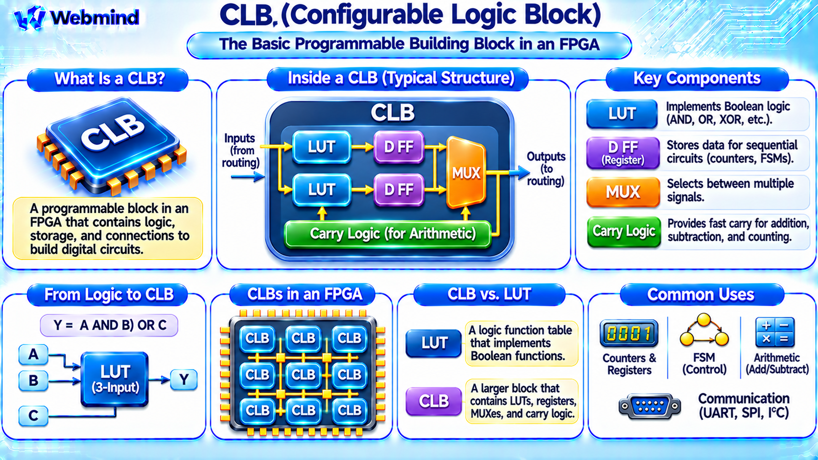
A CLB, or Configurable Logic Block, is a fundamental programmable hardware component inside a Field-Programmable Gate Array (FPGA).
It contains configurable logic resources that allow engineers to implement digital circuits without manufacturing a custom semiconductor chip.
CLBs are used to construct arithmetic circuits, counters, registers, multiplexers, decoders, and Finite State Machines (FSMs).
By combining many CLBs through programmable interconnections, an FPGA can implement complex digital hardware.
A typical CLB contains Look-Up Tables (LUTs), flip-flops, multiplexers, and other supporting logic.
The exact architecture varies between FPGA manufacturers and device families.
How Does a CLB Work?
A CLB provides configurable resources for implementing combinational and sequential logic.
Combinational logic calculates outputs based on current input values, while sequential logic stores information and changes state in response to clock events.
For example, a CLB may use a LUT to implement an AND, OR, or XOR function. A nearby flip-flop can store the result at the next clock edge.
Programmable routing connects the CLB to other logic blocks, memory resources, and input/output interfaces.
The FPGA configuration bitstream determines the functions implemented by the LUTs, the behavior of supported control features, and the connections between resources.
This allows the same physical CLB to perform different hardware functions after reconfiguration.
Main Components of a CLB
A configurable logic block commonly includes several important resources.
Look-Up Tables (LUTs): Implement Boolean functions by storing predefined output values and selecting them according to input signals.
Flip-Flops: Store binary information and support registers, counters, and sequential circuits.
Multiplexers: Select signals and determine how data moves between internal logic resources.
Carry Logic: Provides dedicated paths for efficient arithmetic operations such as addition and counting.
Control Signals: May support clock, reset, set, and clock-enable functions for registers.
Local Interconnections: Connect resources inside the block and provide access to the FPGA’s programmable routing network.
Not every FPGA uses the same CLB organization. Some architectures group several smaller logic elements into one larger configurable block.
What Is a LUT Inside a CLB?
A LUT is one of the main combinational logic resources found in many CLBs.
A LUT with n inputs can implement any single-output Boolean function of those inputs by storing 2ⁿ truth-table values.
For example, a four-input LUT stores sixteen output bits, while a six-input LUT can represent sixty-four output combinations.
A LUT can implement a simple AND gate, XOR gate, multiplexer, or a more complicated Boolean expression.
For example:
Y = (A AND B) OR C
This three-input function can be implemented using a suitable LUT without requiring separate physical AND and OR gates.
Many modern FPGA architectures use six-input LUTs, although supported sizes and configurations depend on the device family.
How Do Flip-Flops Work Inside a CLB?
Flip-flops provide storage for sequential logic.
A D flip-flop captures its input value at a specified clock edge and retains that value until the next update or applicable control event.
Inside a CLB, a LUT can calculate the next value of a digital circuit while a flip-flop stores the current value.
For example, a counter requires combinational logic to calculate the next count and registers to preserve its current count between clock edges.
Some CLBs allow a LUT output to connect directly to a register or bypass the register and feed combinational logic.
This flexibility makes CLBs suitable for both combinational and sequential circuit designs.
What Is Dedicated Carry Logic?
Arithmetic circuits frequently require carry signals to propagate between binary bit positions.
Implementing these connections entirely through general-purpose LUTs and routing can introduce unnecessary delay.
Many FPGAs therefore include dedicated carry-chain resources associated with their logic blocks.
Carry chains provide optimized connections for arithmetic functions such as addition, subtraction, comparison, and counting.
For example, a multi-bit binary adder can use LUTs to calculate selected logic functions while dedicated carry resources propagate carry information efficiently.
This arrangement can improve arithmetic performance and reduce general-purpose routing requirements.
How Are CLBs Connected?
An FPGA contains many programmable logic blocks arranged across the chip.
These blocks are connected through programmable routing resources, including wires, switching structures, and routing channels.
For example, the output of one CLB may become an input to another CLB.
Multiple CLBs can therefore work together to implement circuits larger than a single block can support.
A state machine may use several CLBs for its next-state logic, while registers in the logic blocks store the current state.
Routing flexibility is a major advantage of FPGAs, but routing delays can influence performance.
FPGA implementation tools optimize placement and routing to satisfy timing constraints.
CLB vs. LUT: What Is the Difference?
A LUT and a CLB are related but different concepts.
LUT: A configurable logic resource that implements a Boolean function using stored truth-table values.
CLB: A larger architectural block that contains LUTs, registers, and supporting logic resources.
A CLB may contain multiple LUTs and flip-flops, along with carry logic, selection circuits, and local interconnections.
Therefore, a LUT is usually one component of a CLB rather than another name for the complete block.
The distinction is important when reading FPGA architecture diagrams and resource utilization reports.
CLB vs. DSP Block vs. Block RAM
Modern FPGAs contain specialized resources in addition to configurable logic blocks.
CLB: Implements general-purpose combinational and sequential digital logic.
DSP Block: Performs arithmetic operations such as multiplication, addition, and multiply-accumulate calculations.
Block RAM: Provides dedicated on-chip memory for buffers, FIFOs, and data storage.
For example, a digital signal-processing system may use CLBs for control logic, DSP blocks for arithmetic operations, and Block RAM for storing input samples.
Using specialized resources can reduce CLB consumption and improve hardware efficiency.
What Are CLB Slices?
Some FPGA architectures divide CLBs into smaller organizational units commonly called slices.
A slice typically contains a group of LUTs, registers, and associated logic resources.
For example, AMD FPGA families use slices within configurable logic blocks, although the exact structure differs between architectural generations.
Certain slices may support additional functions such as distributed memory or shift-register logic.
Other FPGA manufacturers use different terminology and organizations.
Intel FPGA devices, for example, use structures such as Adaptive Logic Modules (ALMs) rather than following the same CLB-and-slice arrangement.
These architectural differences influence how synthesis tools map hardware designs onto programmable resources.
CLBs in FPGA Counters and State Machines
CLBs are widely used to implement sequential digital circuits.
Consider a four-bit binary counter.
The current count is stored in four flip-flops, while combinational logic calculates the next count value.
The FPGA implementation tool maps these functions onto available LUTs, registers, and carry resources.
A Finite State Machine operates similarly.
Registers store the current state, LUTs calculate the next state, and output logic generates the required control signals.
Multiple CLBs may be connected to implement larger controllers.
These examples demonstrate how CLBs combine logic processing with state storage.
How Does Verilog Become CLB Hardware?
FPGA designers usually describe circuit behavior using Verilog, SystemVerilog, or VHDL rather than configuring individual CLBs manually.
For example, a designer may write a Verilog description of a counter, decoder, or communication controller.
The FPGA development tools process the design through several stages.
Synthesis: Converts the hardware description into logic functions and sequential elements.
Technology Mapping: Maps the functions onto LUTs, flip-flops, carry chains, and other available FPGA resources.
Placement: Assigns the mapped resources to physical locations inside the FPGA.
Routing: Connects the placed resources through programmable interconnections.
Timing Analysis: Checks whether the implementation satisfies clock and signal timing requirements.
Bitstream Generation: Produces the configuration data used to program the FPGA.
This process allows engineers to create complex circuits without manually assigning every logic function to a particular CLB.
What Is CLB Utilization?
CLB utilization measures how much of an FPGA’s configurable logic capacity is used by a design.
For example, suppose an FPGA contains 10,000 available CLBs and a design occupies 4,000 of them.
The simplified utilization is:
4,000 ÷ 10,000 × 100% = 40%
However, actual FPGA resource reports may separately measure LUTs, registers, slices, logic cells, and other resources.
These measurements are not always interchangeable.
A design may use many registers but relatively few LUTs, or many LUTs but fewer registers.
High logic utilization can also make placement and routing more difficult.
Engineers therefore examine multiple resource and timing metrics rather than relying on CLB count alone.
Why Are CLBs Important for FPGA Performance?
CLBs strongly influence how efficiently a digital design can be implemented.
Important factors include the number of available LUTs, register capacity, carry-chain architecture, local routing, and signal propagation delay.
A design with long combinational paths may require additional pipeline registers to achieve a higher clock frequency.
Similarly, a poorly optimized logic network may consume more LUTs and routing resources than necessary.
EDA tools attempt to balance performance, power consumption, and hardware utilization.
However, overall FPGA performance also depends on Block RAM, DSP resources, clock distribution, external interfaces, and the quality of the hardware design.
Applications of CLBs
CLBs are used throughout FPGA-based digital systems.
Digital Logic: Implement AND, OR, XOR, multiplexers, decoders, and Boolean functions.
Counters and Registers: Store and update binary values.
Finite State Machines: Implement state-transition and control logic.
Communication Interfaces: Support UART, SPI, I2C, and custom digital protocols.
Embedded Controllers: Implement control functions for sensors, motors, and external devices.
Arithmetic Circuits: Build adders, comparators, and selected processing operations.
Hardware Accelerators: Provide custom control and data-processing logic for specialized applications.
These applications demonstrate the flexibility of configurable logic blocks.
Advantages and Limitations of CLBs
The main advantage of a CLB is its programmability.
The same physical resources can implement many different digital functions, allowing hardware designs to be changed without manufacturing a new chip.
CLBs also combine logic and storage resources, making them useful for implementing complete synchronous digital circuits.
However, programmable hardware introduces additional routing, configuration, and timing overhead compared with some fixed-function ASIC implementations.
Complex arithmetic and memory operations may also be more efficient when implemented using dedicated DSP blocks or Block RAM.
FPGA designers therefore combine CLBs with specialized resources to achieve the required performance and efficiency.
Conclusion
A Configurable Logic Block is a fundamental programmable hardware structure inside an FPGA.
It combines resources such as LUTs, flip-flops, multiplexers, carry logic, and local interconnections to implement digital circuits.
Multiple CLBs are connected through programmable routing to build larger systems, including counters, state machines, arithmetic circuits, and communication controllers.
Although FPGA architectures differ between manufacturers, configurable logic blocks remain central to the flexibility of programmable hardware.
Understanding CLBs provides an important foundation for studying FPGA architecture, LUTs, flip-flops, Boolean algebra, Verilog, logic synthesis, and digital circuit design.