Introduction
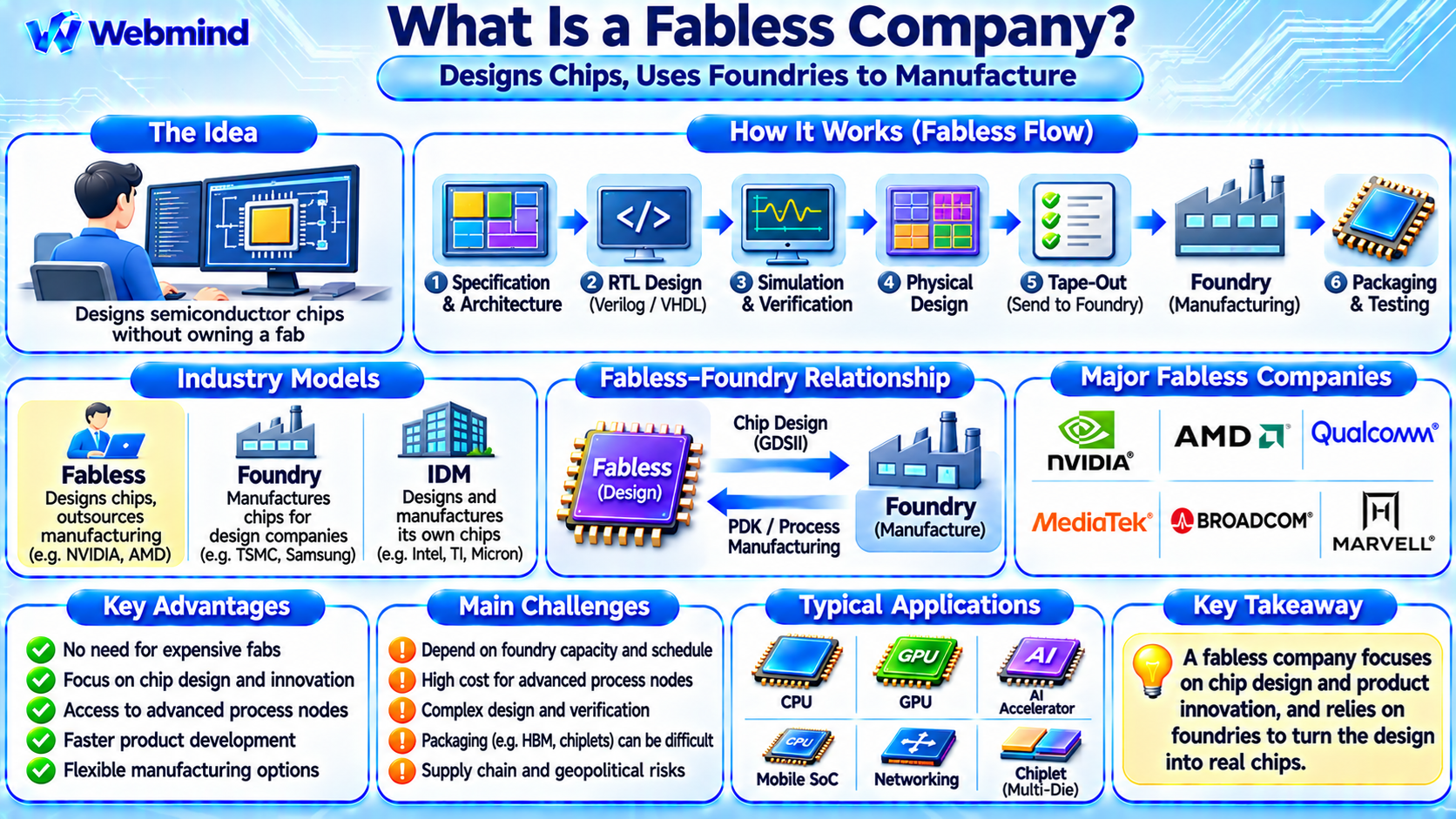
A fabless semiconductor company is a company that designs and develops semiconductor chips but outsources their physical manufacturing to specialized semiconductor foundries.
The word fabless means “without a fabrication plant.”
Instead of owning expensive semiconductor manufacturing facilities, fabless companies focus on chip architecture, circuit design, verification, software development, and product innovation.
Well-known fabless semiconductor companies include NVIDIA, AMD, Qualcomm, MediaTek, Broadcom, and Marvell.
The fabless business model has become a major part of the semiconductor industry, supporting the development of CPUs, GPUs, smartphone processors, AI accelerators, networking chips, and many other integrated circuits.
How Does a Fabless Semiconductor Company Work?
A fabless company begins by defining the requirements of a semiconductor product.
Engineers develop the chip architecture, design digital and analog circuits, and use Electronic Design Automation (EDA) software to simulate and verify the design.
Once the chip design is completed, the company selects a semiconductor foundry to manufacture it.
The foundry uses specialized equipment and manufacturing processes to fabricate the circuits on silicon wafers.
After manufacturing, the chips undergo testing, packaging, and additional validation before being delivered to customers.
The fabless company remains responsible for product development, performance, functionality, and commercial success, even though manufacturing is performed by external partners.
Main Stages of Fabless Chip Development
1. Chip Architecture and Specification
The development process begins with defining the chip’s intended functions, performance requirements, power consumption, and target applications.
For example, an AI accelerator may require specialized matrix-processing units, high memory bandwidth, and efficient communication interfaces.
Engineers translate these requirements into a detailed hardware architecture.
2. RTL and Circuit Design
Digital hardware engineers describe circuit behavior using Hardware Description Languages (HDLs), such as Verilog, SystemVerilog, or VHDL.
Analog and mixed-signal engineers use circuit schematics, transistor models, and specialized simulation tools.
The resulting designs define the hardware functions that will eventually be implemented in silicon.
3. Simulation and Verification
Before manufacturing, engineers verify that the design behaves correctly.
EDA tools perform functional simulation, formal verification, timing analysis, and other checks.
This stage is extremely important because correcting a design error after manufacturing can be expensive.
4. Physical Design
The logical design is transformed into a physical layout containing transistor-level structures and electrical interconnections.
EDA tools perform synthesis, placement, routing, timing optimization, and physical verification.
The design must follow the manufacturing rules provided by the selected foundry.
5. Tape-Out and Manufacturing
Tape-out is the milestone when the completed chip layout is delivered for semiconductor manufacturing.
The foundry uses processes such as photolithography, deposition, etching, ion implantation, and metallization to manufacture the integrated circuits on silicon wafers.
The resulting wafers contain many individual semiconductor dies.
6. Packaging, Testing, and Product Delivery
After fabrication, the dies are tested, separated, and packaged.
Packaging and testing may be performed by the foundry, an outsourced assembly and test provider, or other manufacturing partners.
The fabless company then validates the finished chips and prepares them for commercial products.
Fabless vs. Foundry vs. IDM
Three major business models are commonly used in the semiconductor industry.
Fabless Company: Designs semiconductor chips but outsources wafer manufacturing. Examples include NVIDIA, AMD, Qualcomm, and MediaTek.
Foundry: Manufactures semiconductor chips for external customers using specialized fabrication facilities. Examples include TSMC, GlobalFoundries, UMC, and Samsung Foundry.
Integrated Device Manufacturer (IDM): Designs and manufactures its own semiconductor products. Examples include Intel, Texas Instruments, and Micron.
These categories are not always exclusive.
For example, an IDM may outsource some manufacturing to external foundries, while a company operating its own fabs may also offer foundry services to other semiconductor designers.
Why Do Fabless Companies Use Foundries?
Advanced semiconductor manufacturing requires enormous capital investment.
Modern fabrication facilities use highly specialized lithography, deposition, etching, inspection, and testing equipment.
Leading-edge semiconductor fabs can require investments reaching tens of billions of dollars.
Building a fab also requires highly skilled engineers, reliable electricity, ultrapure water, specialized materials, and continuous manufacturing process development.
By outsourcing fabrication, fabless companies avoid owning and operating these facilities.
Instead, they can concentrate their resources on chip architecture, design, verification, product development, and customer requirements.
This separation allows specialized design companies and manufacturing companies to develop expertise in their respective areas.
Major Fabless Semiconductor Companies
NVIDIA
NVIDIA designs GPUs, AI accelerators, networking processors, and related computing technologies.
Its products are widely used in gaming, artificial intelligence, data centers, scientific computing, and professional graphics.
NVIDIA relies on external semiconductor manufacturing and packaging partners to produce its chips.
AMD
AMD develops CPUs, GPUs, adaptive computing products, and data center processors.
Its Ryzen and EPYC processor families use advanced semiconductor architectures, including chiplet-based designs.
AMD outsources semiconductor fabrication to manufacturing partners rather than operating its own leading-edge wafer fabs.
Qualcomm
Qualcomm develops mobile processors, wireless communication chips, and other semiconductor technologies.
Its Snapdragon platforms combine CPU, GPU, AI, communication, and multimedia capabilities.
Qualcomm primarily uses external foundries for semiconductor production.
MediaTek
MediaTek designs processors and communication chips for smartphones, smart televisions, networking devices, and other electronic products.
It is a major supplier of highly integrated Systems-on-Chip (SoCs).
Broadcom and Marvell
Broadcom and Marvell develop semiconductor solutions for networking, data centers, communications, storage, and specialized computing applications.
Their products include high-speed networking chips, communication processors, and custom silicon solutions.
These companies demonstrate how the fabless model supports different areas of computing and electronics.
What Is the Relationship Between Fabless Companies and TSMC?
TSMC, or Taiwan Semiconductor Manufacturing Company, is a major dedicated semiconductor foundry.
Many fabless semiconductor companies use TSMC to manufacture their chips.
A fabless company provides the design, while TSMC supplies manufacturing technology and wafer fabrication services.
The foundry also provides process-related information through Process Design Kits (PDKs), enabling designers to create circuits compatible with specific manufacturing technologies.
For example, a fabless company may design a processor using an advanced FinFET or GAAFET manufacturing process offered by a foundry.
The company and foundry must coordinate design rules, manufacturing constraints, testing requirements, and production schedules.
This collaboration is an important part of modern semiconductor development.
What Are EDA Tools and IP Cores?
Fabless companies rely heavily on Electronic Design Automation tools and reusable semiconductor intellectual property.
EDA Tools: Software used for circuit design, simulation, logic synthesis, physical implementation, timing analysis, and verification.
IP Cores: Pre-designed hardware components that can be integrated into larger chip designs.
Common IP blocks include CPU cores, memory controllers, PCI Express interfaces, USB controllers, and communication circuits.
For example, a fabless company developing a mobile SoC may license CPU architecture or processor IP from Arm while designing additional hardware components internally.
Using verified IP blocks can reduce development time and engineering risk.
However, licensed IP must still be integrated, configured, and verified within the complete chip design.
Advantages of the Fabless Business Model
Lower Manufacturing Capital Requirements: Fabless companies do not need to build and operate semiconductor wafer fabrication facilities.
Focus on Innovation: Engineering resources can concentrate on architecture, circuit design, software, and product development.
Access to Advanced Processes: Companies can use manufacturing technologies developed by specialized foundries.
Business Flexibility: Fabless companies may select different foundries or process nodes for different products when technically and commercially feasible.
Faster Market Entry: New semiconductor design companies can develop products without first establishing a manufacturing operation.
Specialization: Foundries and design companies can focus on their respective technical strengths.
These advantages have helped the fabless model become important throughout the semiconductor industry.
Challenges of Fabless Semiconductor Companies
Despite its benefits, the fabless model also introduces several challenges.
Manufacturing Dependence: Production depends on external foundries and their available capacity.
Supply Chain Risks: Manufacturing delays, equipment shortages, or geopolitical disruptions can affect product availability.
Advanced Process Costs: Leading-edge manufacturing remains expensive even without owning a fab.
Design Complexity: Modern chips require large engineering teams, advanced EDA tools, and extensive verification.
Packaging Requirements: AI accelerators and chiplet-based processors may require sophisticated packaging and HBM integration.
Production Scheduling: Fabless companies must coordinate manufacturing capacity, packaging, testing, and product delivery.
Technology Access: Not every foundry offers the same process technologies, intellectual property, or manufacturing capabilities.
Successful fabless companies therefore need strong engineering capabilities and reliable relationships with manufacturing partners.
Fabless Companies and Advanced Chiplets
Chiplet technology is especially relevant to modern fabless semiconductor design.
Instead of creating one large monolithic chip, engineers can divide a processor into several smaller semiconductor dies.
For example, a processor may contain separate compute chiplets and an input/output die.
These components may be manufactured using different process nodes and assembled through advanced semiconductor packaging.
This approach allows designers to optimize different functions independently.
It can also improve manufacturing flexibility and potentially reduce certain costs associated with very large monolithic dies.
However, chiplet architectures introduce additional complexity involving interconnect bandwidth, power delivery, latency, thermal management, and packaging.
Fabless Companies and Artificial Intelligence
Artificial intelligence has increased demand for specialized semiconductor processors.
Fabless companies design GPUs, NPUs, AI accelerators, networking chips, and other components used in AI computing systems.
These chips often require advanced process nodes, high memory bandwidth, and sophisticated packaging technologies.
For example, large AI accelerators may combine computing dies with multiple High Bandwidth Memory (HBM) stacks.
Manufacturing such devices requires cooperation among chip designers, foundries, memory manufacturers, and advanced packaging providers.
The fabless model allows companies to focus on computing architecture and AI hardware innovation while relying on specialized partners for production.
Why Is the Fabless Model Important?
The fabless business model has helped reshape the global semiconductor industry.
It allows companies to specialize in chip design while foundries concentrate on manufacturing technologies and production efficiency.
This division has supported the development of complex processors, high-performance graphics chips, mobile SoCs, networking ASICs, and AI accelerators.
It has also enabled smaller semiconductor companies to enter specialized markets without building expensive fabrication facilities.
However, the success of the model depends on a complex network of foundries, EDA providers, IP suppliers, packaging companies, and testing facilities.
Modern chip development is therefore often a collaboration among several specialized organizations.
Conclusion
A fabless semiconductor company designs integrated circuits but relies on external foundries to manufacture them.
Companies such as NVIDIA, AMD, Qualcomm, MediaTek, Broadcom, and Marvell demonstrate the importance of this business model in modern computing.
Fabless companies focus on architecture, RTL design, verification, physical design, and product development, while foundries perform wafer fabrication.
This specialization can reduce capital requirements and provide access to advanced semiconductor manufacturing technologies.
Understanding the fabless model is essential for studying semiconductor foundries, EDA, chip design, process nodes, ASICs, chiplets, and the global semiconductor supply chain.