Introduction
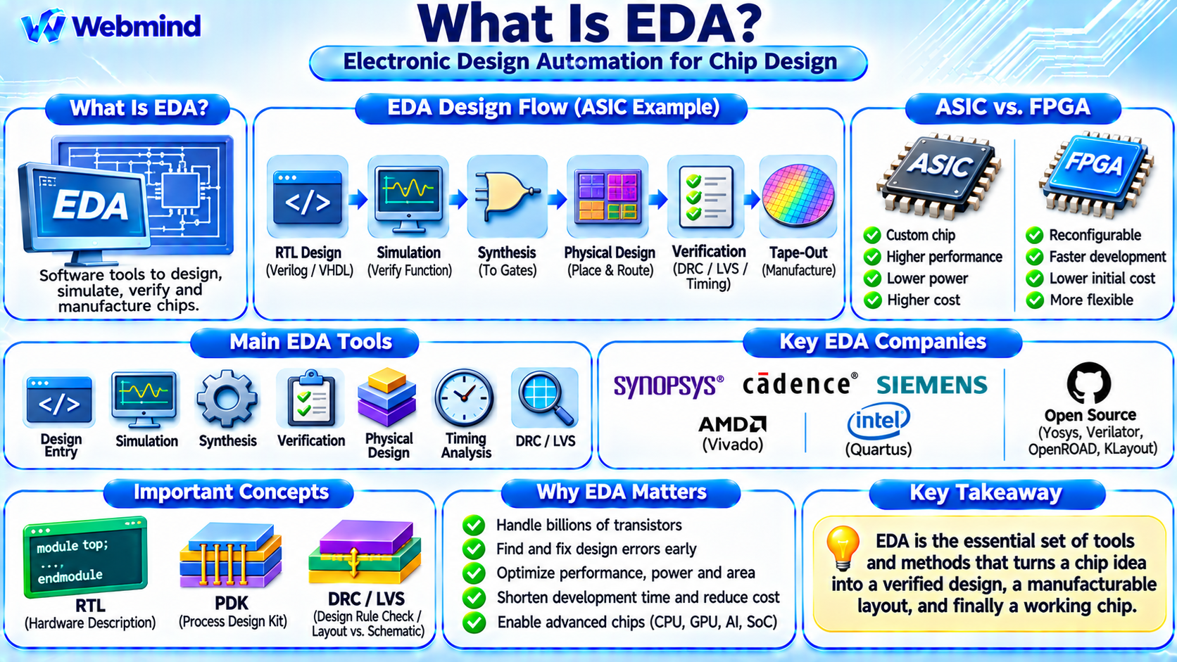
EDA, or Electronic Design Automation, refers to software tools and methodologies used to design, simulate, verify, and manufacture electronic circuits and semiconductor chips.
EDA is essential for developing modern CPUs, GPUs, FPGAs, ASICs, microcontrollers, and Systems-on-Chip (SoCs).
Modern integrated circuits can contain billions of transistors and extremely complex electrical connections. Designing such circuits manually would be impractical.
EDA tools automate many engineering tasks, including circuit simulation, logic synthesis, physical design, timing analysis, power optimization, and design verification.
The semiconductor industry relies heavily on EDA technology to transform circuit ideas into working hardware.
How Does EDA Work?
EDA provides an integrated workflow that allows engineers to move from a circuit specification to a physical implementation.
For example, a digital chip designer may begin by describing a processor or hardware controller using a Hardware Description Language (HDL), such as Verilog, SystemVerilog, or VHDL.
EDA software can simulate the design to check its behavior, convert the description into logic gates, and determine how those gates should be physically connected.
For ASIC manufacturing, additional tools arrange the logic cells on silicon, route electrical connections, analyze timing, and verify that the layout follows semiconductor manufacturing rules.
For FPGA development, EDA tools map the design onto programmable logic resources and generate a configuration bitstream.
Although these workflows share many concepts, ASICs and FPGAs require different implementation processes.
Main Categories of EDA Tools
EDA software includes several important categories.
Design Entry Tools: Allow engineers to describe circuits using schematic diagrams, HDLs, or higher-level design languages.
Simulation Tools: Test circuit behavior before hardware is manufactured or programmed.
Logic Synthesis Tools: Convert RTL descriptions into networks of logic gates or FPGA resources.
Verification Tools: Check whether a design behaves according to its specifications.
Physical Design Tools: Arrange standard cells and connect them through metal routing layers.
Static Timing Analysis Tools: Evaluate whether circuit paths satisfy required timing constraints.
Power Analysis Tools: Estimate or analyze electrical power consumption.
Physical Verification Tools: Check manufacturing design rules and the relationship between circuit layout and intended connectivity.
These tools work together to identify problems before they become expensive hardware failures.
What Is RTL Design?
RTL stands for Register Transfer Level.
RTL design describes how data moves between registers and how combinational logic processes that data.
Engineers commonly write RTL using Verilog, SystemVerilog, or VHDL.
For example, a designer may describe a counter that increments its stored value on each clock cycle.
The RTL specifies the required behavior without manually drawing every transistor or logic gate.
EDA synthesis tools interpret the RTL and produce a hardware implementation using available logic resources.
RTL is widely used for processor cores, memory controllers, communication interfaces, and digital signal processing circuits.
What Is Logic Synthesis?
Logic synthesis converts a hardware description into a lower-level representation suitable for implementation.
For ASIC designs, the synthesis tool typically maps logic into standard cells provided by a semiconductor manufacturing library.
These cells may implement NAND gates, flip-flops, multiplexers, adders, and other functions.
For FPGA designs, synthesis and technology mapping convert logic into resources such as Look-Up Tables (LUTs), registers, block RAM, and DSP blocks.
Synthesis tools optimize the implementation according to constraints involving timing, area, and power consumption.
However, synthesis does not guarantee that a design is functionally correct. Simulation and verification remain essential.
What Is Functional Verification?
Functional verification checks whether an electronic design performs the operations required by its specification.
A design may contain logically incorrect behavior even when its source code is syntactically valid.
EDA verification techniques include several approaches.
RTL Simulation: Executes the hardware description using test inputs and checks the resulting outputs.
Testbenches: Provide input stimuli, expected results, and checking mechanisms.
Assertions: Express properties that must hold during circuit operation.
Formal Verification: Uses mathematical methods to prove or disprove selected design properties.
Hardware Emulation: Uses specialized hardware to execute large digital designs at higher speeds than conventional software simulation in many situations.
Verification is one of the most important and resource-intensive parts of semiconductor design.
Finding a functional error before manufacturing is far less expensive than discovering it after silicon fabrication.
What Is Physical Design?
Physical design converts a logical circuit into a physical layout that can be manufactured on silicon.
This process is particularly important for ASIC development.
Several major stages are involved.
Floorplanning: Defines the overall chip organization, including major functional blocks, memory arrays, and input/output regions.
Placement: Determines the physical locations of standard cells within the chip layout.
Clock Tree Synthesis (CTS): Builds clock distribution networks to deliver timing signals to sequential circuit elements.
Routing: Creates the metal interconnections that connect circuit components.
Timing Optimization: Adjusts the implementation to satisfy timing requirements.
Power Optimization: Helps reduce unnecessary switching power, leakage, and other energy losses.
The output is a physical layout containing the geometric information required for semiconductor manufacturing.
What Is Static Timing Analysis?
Static Timing Analysis (STA) is an EDA technique used to evaluate the timing characteristics of digital circuits without simulating every possible input sequence.
STA analyzes signal propagation delays through combinational logic and interconnections.
It checks whether signals arrive at registers within the required timing windows.
Two important timing requirements are setup time and hold time.
Setup Time: The input data must remain stable for a specified interval before the active clock edge.
Hold Time: The input data must remain stable for a specified interval after the active clock edge.
Timing analysis also accounts for clock skew, circuit delays, operating conditions, and manufacturing variation.
STA is essential for determining whether a digital circuit can operate reliably at its intended clock frequency.
What Are DRC and LVS?
Before an ASIC layout is sent for manufacturing, engineers perform physical verification.
Two important verification methods are Design Rule Checking (DRC) and Layout Versus Schematic (LVS).
DRC: Checks whether the physical layout follows the manufacturing rules specified by the semiconductor foundry. These rules include minimum spacing, width, enclosure, and other geometric requirements.
LVS: Compares the electrical connectivity extracted from the physical layout against the intended circuit netlist.
DRC helps ensure that the layout is manufacturable, while LVS helps ensure that the manufactured circuit will match the intended logical design.
Both are critical stages before tape-out.
What Is Tape-Out?
Tape-out is the milestone at which an integrated circuit design is finalized and delivered for semiconductor manufacturing.
Before tape-out, engineers complete extensive functional verification, timing analysis, power checks, and physical verification.
The final design data is typically delivered using formats such as GDSII or OASIS.
The semiconductor foundry uses this layout information, along with other manufacturing data, to prepare the photomasks and fabrication process.
After fabrication, the resulting chips undergo testing and validation.
A design error discovered after tape-out may require another manufacturing cycle, which can be extremely expensive.
EDA for FPGA Development
FPGA development relies on EDA tools, but the workflow differs from ASIC manufacturing.
A typical FPGA design process includes:
HDL Design: Describe the required digital circuit using Verilog, SystemVerilog, or VHDL.
Simulation: Verify circuit functionality before implementation.
Synthesis: Convert the RTL into logic suitable for the target FPGA.
Placement and Routing: Map the design onto the FPGA’s configurable logic blocks, registers, routing networks, and specialized resources.
Timing Analysis: Check whether the implemented circuit satisfies the required timing constraints.
Bitstream Generation: Produce the configuration data used to program the FPGA.
Hardware Testing: Load the design onto an FPGA board and verify its behavior.
Because an FPGA is reconfigurable, developers can modify and test designs without manufacturing a new semiconductor chip.
Popular FPGA design environments include AMD Vivado, Intel Quartus Prime, and other vendor-specific tools.
EDA for ASIC vs. FPGA
ASIC and FPGA development share concepts such as RTL design, simulation, synthesis, and timing verification.
However, their final implementation methods are different.
ASIC EDA: Produces a physical integrated circuit layout for semiconductor fabrication. It requires foundry technology files, standard-cell libraries, physical verification, and tape-out.
FPGA EDA: Produces a configuration bitstream for an existing programmable semiconductor device. The FPGA’s transistors and routing resources are already manufactured.
ASIC designs can achieve excellent performance, power efficiency, and area optimization for specific applications, but manufacturing involves significant cost and long development cycles.
FPGA designs provide flexibility and faster hardware iteration but are constrained by the resources and architecture of the selected device.
Who Develops EDA Software?
Several companies and open-source projects provide EDA tools.
Synopsys: Develops tools for logic synthesis, simulation, static timing analysis, physical implementation, and semiconductor design verification.
Cadence Design Systems: Provides EDA technologies for digital design, verification, analog circuit design, physical implementation, and system analysis.
Siemens EDA: Offers tools for functional verification, physical verification, design-for-test, and other semiconductor engineering tasks.
AMD and Intel: Provide FPGA development environments for their programmable logic devices.
Open-Source EDA: Projects such as Yosys, Verilator, OpenROAD, and KLayout support different parts of digital design, simulation, synthesis, physical implementation, and layout analysis.
Different EDA products serve different stages of the design workflow, and no single tool performs every engineering task.
What Is a Process Design Kit?
A Process Design Kit (PDK) is a collection of technology information provided or authorized by a semiconductor foundry.
It allows chip designers to create circuits compatible with a specific manufacturing process.
A PDK may contain transistor models, manufacturing design rules, layer definitions, device layouts, and other technology-specific information.
EDA tools use these files for simulation, layout design, parasitic extraction, and physical verification.
Advanced semiconductor process nodes require highly detailed PDKs because transistor characteristics and manufacturing constraints are extremely complex.
PDKs connect electronic circuit design with the practical requirements of semiconductor manufacturing.
Why Is EDA Important?
EDA makes modern semiconductor design possible.
Without EDA, engineers would struggle to manage the enormous complexity of advanced integrated circuits.
EDA software helps improve design productivity, detect errors, optimize performance, and reduce development risks.
It also allows engineers to explore different circuit architectures before committing to hardware.
Modern EDA increasingly incorporates machine learning and optimization techniques to assist with tasks such as floorplanning, placement, routing, verification, and power-performance-area optimization.
However, automated tools still require accurate specifications, engineering judgment, and thorough validation.
Challenges of Modern EDA
As semiconductor technology advances, EDA faces increasingly difficult problems.
Design Complexity: Modern SoCs may contain billions of transistors and many interacting hardware blocks.
Advanced Process Nodes: Smaller devices introduce more complicated manufacturing and electrical constraints.
Power Consumption: Engineers must optimize performance while limiting energy use and heat generation.
Verification Complexity: Large hardware systems have enormous numbers of possible operating states.
Chiplet Integration: Multi-die systems require coordinated electrical, thermal, and communication design.
Development Cost: Advanced commercial EDA tools and semiconductor engineering resources can be expensive.
These challenges continue to drive improvements in design automation technology.
Conclusion
Electronic Design Automation is the collection of software tools and engineering methods used to design, simulate, verify, and implement electronic circuits.
EDA connects hardware descriptions with physical semiconductor manufacturing or FPGA configuration.
Important EDA stages include RTL design, simulation, logic synthesis, timing analysis, physical design, and verification.
Commercial platforms from Synopsys, Cadence, Siemens, and FPGA manufacturers work alongside open-source tools to support modern hardware development.
Understanding EDA is essential for studying digital logic, Verilog, FPGA design, ASIC development, semiconductor manufacturing, and modern computer architecture.