Introduction
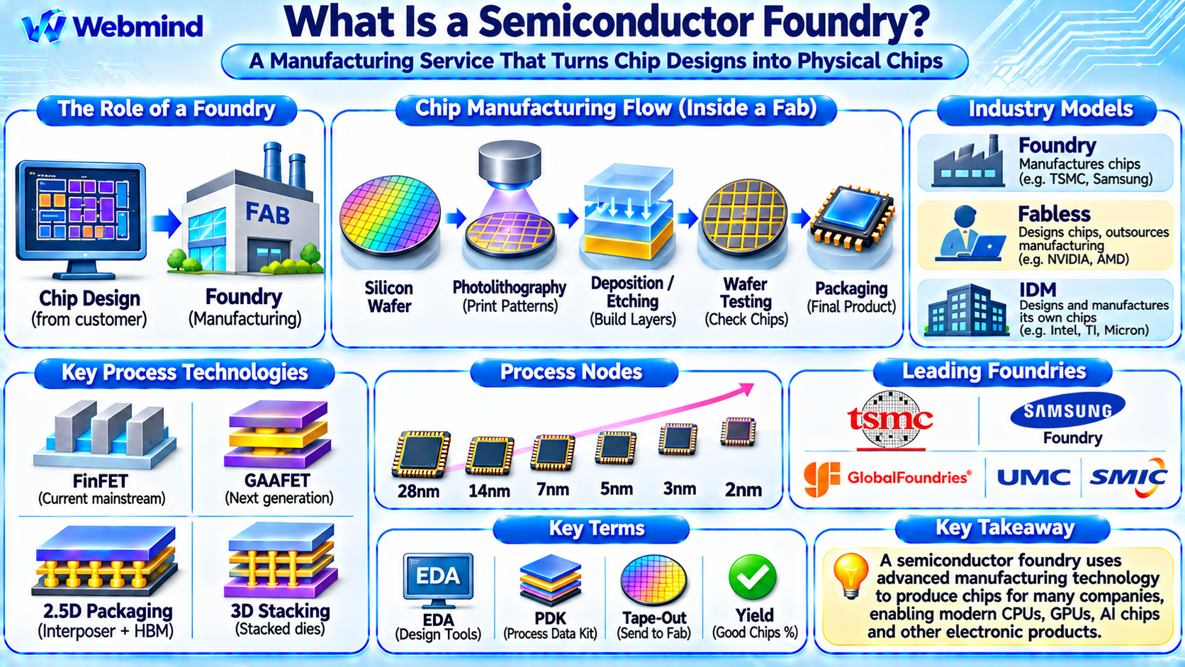
A semiconductor foundry is a company or manufacturing facility that produces semiconductor chips based on circuit designs.
Foundries use highly specialized equipment and manufacturing processes to fabricate integrated circuits on silicon wafers.
Modern CPUs, GPUs, memory-related circuits, microcontrollers, FPGAs, ASICs, and artificial intelligence accelerators depend on advanced semiconductor manufacturing.
Many semiconductor companies design chips without owning their own manufacturing facilities.
These companies, known as fabless semiconductor companies, rely on foundries to manufacture their designs.
Well-known semiconductor foundries include TSMC, Samsung Foundry, GlobalFoundries, UMC, and SMIC.
Foundries are an essential part of the global semiconductor supply chain because they transform digital chip designs into physical silicon devices.
How Does a Semiconductor Foundry Work?
A foundry receives a completed chip design from a semiconductor design company.
The design contains detailed information describing the transistors, circuit structures, and electrical interconnections that must be manufactured.
Before manufacturing, engineers use a Process Design Kit (PDK) to ensure the design is compatible with the foundry’s manufacturing technology.
After the design passes the required verification stages, the final layout is delivered for production through a process called tape-out.
The foundry then manufactures the integrated circuits on silicon wafers using repeated fabrication processes.
These include photolithography, deposition, etching, ion implantation, and thermal processing.
After fabrication, the wafers undergo inspection and electrical testing.
Individual dies are subsequently separated and packaged, either through the foundry’s own services or through specialized packaging companies.
Foundry vs. Fabless vs. IDM
The semiconductor industry uses several different business models.
Foundry
A foundry primarily manufactures semiconductor chips for other companies.
Its customers provide chip designs, while the foundry supplies manufacturing technology, fabrication facilities, and production expertise.
TSMC is a prominent example of a dedicated semiconductor foundry.
Fabless Semiconductor Company
A fabless company designs semiconductor chips but generally outsources wafer manufacturing.
Examples include NVIDIA, AMD, Qualcomm, and many other semiconductor design companies.
Fabless companies focus on processor architecture, circuit design, product development, and software ecosystems.
Integrated Device Manufacturer (IDM)
An Integrated Device Manufacturer designs and manufactures semiconductor products within the same company.
Intel, Texas Instruments, and Micron are examples of companies with substantial internal semiconductor manufacturing operations.
Some IDMs also use external foundries for selected products or provide manufacturing services to outside customers.
These business models can overlap as semiconductor companies adopt more flexible manufacturing strategies.
What Happens Inside a Semiconductor Fab?
A semiconductor fabrication facility, commonly called a fab, contains extremely sophisticated manufacturing equipment.
Chip fabrication begins with highly purified silicon wafers.
The wafers pass through hundreds or thousands of individual processing operations, depending on the manufacturing technology.
Photolithography: Transfers microscopic circuit patterns onto wafers using light-sensitive materials.
Deposition: Adds thin films of semiconductor, insulating, or conducting materials.
Etching: Removes selected materials to form the required structures.
Ion Implantation: Introduces controlled impurities into semiconductor regions to modify electrical properties.
Thermal Processing: Uses carefully controlled heating to activate dopants and modify material characteristics.
Chemical Mechanical Polishing (CMP): Produces extremely flat surfaces during multi-layer manufacturing.
Metallization: Creates multiple levels of conductive interconnections between transistors and other circuit elements.
These processes are repeated to manufacture the transistors, memory structures, and wiring required for complex integrated circuits.
What Is a Semiconductor Process Node?
A process node describes a generation of semiconductor manufacturing technology.
Common node names include 28nm, 14nm, 7nm, 5nm, 3nm, and 2nm.
Historically, these names were associated with physical transistor dimensions. Today, they primarily describe generations of manufacturing technology rather than one exact physical measurement.
Advanced process nodes combine improvements in transistor architecture, lithography, materials, circuit density, and power efficiency.
For example, FinFET transistors replaced conventional planar MOSFETs in many advanced logic processes.
Newer manufacturing technologies increasingly use Gate-All-Around Field-Effect Transistors (GAAFETs) to improve control over very small semiconductor channels.
Different foundries use different process technologies and naming conventions, so similarly named nodes are not necessarily identical.
Why Are Semiconductor Fabs So Expensive?
Building and operating a semiconductor fab requires enormous financial investment.
Advanced facilities can cost tens of billions of dollars, depending on their capacity and technology.
Several factors contribute to these costs.
Manufacturing Equipment: Lithography, deposition, etching, inspection, and metrology systems require highly specialized engineering.
Cleanroom Infrastructure: Semiconductor production requires extremely controlled environments to minimize contamination.
Research and Development: Advanced process nodes require extensive development of materials, transistors, and manufacturing techniques.
Utilities: Fabs consume significant amounts of electricity, ultrapure water, and industrial gases.
Process Control: Manufacturing requires continuous monitoring of defects, material properties, and process variations.
Skilled Workforce: Semiconductor production depends on engineers and technicians specializing in physics, materials science, chemistry, electronics, and automation.
These requirements create substantial technical and financial barriers to entering the semiconductor manufacturing industry.
What Is Semiconductor Yield?
Yield measures how many manufactured semiconductor dies meet the required functional and quality specifications.
For example, if a wafer contains 500 complete dies and 450 pass testing, the simplified functional yield is 90%.
Manufacturing yield is influenced by several factors, including defect density, die size, process variation, equipment performance, and circuit design.
Advanced semiconductor nodes can be particularly challenging because extremely small features require precise manufacturing control.
A foundry must continually improve its processes to reduce defects and increase the percentage of usable chips.
High yield is economically important because each wafer requires significant materials, equipment time, and processing resources.
Leading Semiconductor Foundries
Several companies play important roles in global semiconductor manufacturing.
TSMC
Taiwan Semiconductor Manufacturing Company (TSMC) is a major dedicated semiconductor foundry.
It manufactures chips for customers across computing, mobile devices, networking, automotive electronics, and artificial intelligence.
TSMC offers both advanced and mature process technologies and provides sophisticated packaging services.
Samsung Foundry
Samsung Foundry manufactures logic semiconductor chips using advanced and mature process technologies.
It has developed technologies involving FinFETs, GAAFETs, and advanced semiconductor packaging.
Samsung also operates major semiconductor memory businesses, although those activities are distinct from its foundry services.
GlobalFoundries
GlobalFoundries focuses on specialized and differentiated semiconductor manufacturing technologies.
Its offerings serve applications such as radio-frequency electronics, automotive systems, industrial devices, communications, and embedded computing.
UMC
United Microelectronics Corporation (UMC) is a semiconductor foundry with significant manufacturing capabilities in mature and specialty process nodes.
It supports a wide range of consumer, industrial, networking, and automotive semiconductor products.
SMIC
Semiconductor Manufacturing International Corporation (SMIC) is a major semiconductor foundry based in China.
It manufactures integrated circuits using a range of semiconductor process technologies.
Its development and production capabilities are influenced by manufacturing equipment availability, technology requirements, and international trade restrictions.
Foundries differ in manufacturing capabilities, process specialization, production capacity, geographic footprint, and customer requirements.
What Is the Role of EDA and PDKs?
Electronic Design Automation (EDA) tools are essential for designing chips that can be manufactured by foundries.
Engineers use EDA software to create circuits, perform logic synthesis, verify functionality, analyze timing, and generate physical layouts.
A foundry provides or authorizes a Process Design Kit (PDK) containing technology-specific information.
The PDK may include transistor models, design rules, electrical parameters, and manufacturing layer definitions.
EDA tools use this information to help ensure that a chip design follows the requirements of the selected process node.
Before tape-out, the design must pass checks such as Design Rule Checking (DRC) and Layout Versus Schematic (LVS).
These verification steps help reduce manufacturing errors and improve the likelihood that fabricated chips will function correctly.
Foundries and Advanced Semiconductor Packaging
Modern foundries increasingly participate in advanced semiconductor packaging and integration.
Traditional semiconductor manufacturing focused heavily on producing individual monolithic dies.
Today, high-performance processors may combine multiple chiplets, stacked memory, and specialized accelerators within one package.
Advanced packaging technologies include 2.5D integration, 3D stacking, silicon interposers, and hybrid bonding.
For example, a high-performance AI accelerator may combine a computing die with multiple High Bandwidth Memory (HBM) stacks.
These components can be connected through advanced packaging technologies that provide very high interconnect bandwidth.
Foundries and specialized assembly companies work together to support these complex products.
Packaging has therefore become an increasingly important part of the semiconductor manufacturing ecosystem.
What Are Specialty Foundries?
Not every semiconductor application requires the most advanced process node.
Many electronic products depend on mature and specialized manufacturing technologies.
Analog and Mixed-Signal Chips: Require carefully controlled electrical characteristics for amplifiers, converters, and communication circuits.
Power Semiconductors: Focus on voltage handling, current capacity, switching efficiency, and reliability.
Automotive Chips: Often require long-term reliability, qualification, and stable manufacturing availability.
RF Semiconductors: Use specialized processes for radio-frequency communication applications.
Embedded Systems: Microcontrollers and industrial processors may prioritize cost, integrated peripherals, and long product lifetimes.
Specialty foundries provide manufacturing processes optimized for these requirements.
Mature process nodes remain economically important even as advanced semiconductor technologies continue to evolve.
Why Are Foundries Important to the Semiconductor Industry?
Foundries allow semiconductor design companies to develop advanced products without building their own expensive manufacturing facilities.
This separation between chip design and manufacturing has helped create a large ecosystem of specialized companies.
It also allows designers to select manufacturing technologies based on performance, cost, power consumption, and production requirements.
Foundries support innovation in artificial intelligence, cloud computing, telecommunications, automotive electronics, robotics, and consumer devices.
However, semiconductor manufacturing also depends on complex global supply chains involving equipment manufacturers, materials suppliers, design software companies, and packaging providers.
Manufacturing capacity, geographic concentration, and access to advanced equipment can therefore influence the availability and cost of semiconductor products.
Challenges Facing Semiconductor Foundries
Semiconductor foundries face several major challenges.
Rising Manufacturing Costs: Advanced process nodes require increasingly expensive equipment and infrastructure.
Technology Complexity: Smaller transistor structures demand more precise manufacturing and verification.
Yield Optimization: Defects and process variations can significantly affect manufacturing economics.
Supply Chain Dependencies: Fabs depend on specialized equipment, chemicals, gases, wafers, and replacement parts.
Energy and Water Requirements: Semiconductor manufacturing requires reliable infrastructure and extensive resource management.
Production Capacity: Building new manufacturing capacity takes substantial time and investment.
Geopolitical Risks: Trade restrictions, export controls, and regional supply-chain disruptions can affect manufacturing operations.
These challenges make long-term planning and technological investment essential for foundry operators.
Conclusion
A semiconductor foundry is a specialized manufacturer that transforms integrated circuit designs into physical semiconductor chips.
Foundries use processes such as photolithography, deposition, etching, ion implantation, and metallization to build transistors and interconnections on silicon wafers.
Companies such as TSMC, Samsung Foundry, GlobalFoundries, UMC, and SMIC serve different parts of the semiconductor market.
The foundry business model allows fabless companies to focus on chip design while relying on specialized manufacturing expertise.
Understanding semiconductor foundries provides an important foundation for studying silicon wafers, process nodes, EDA, chiplets, semiconductor packaging, CPU and GPU manufacturing, and the global semiconductor industry.