Introduction
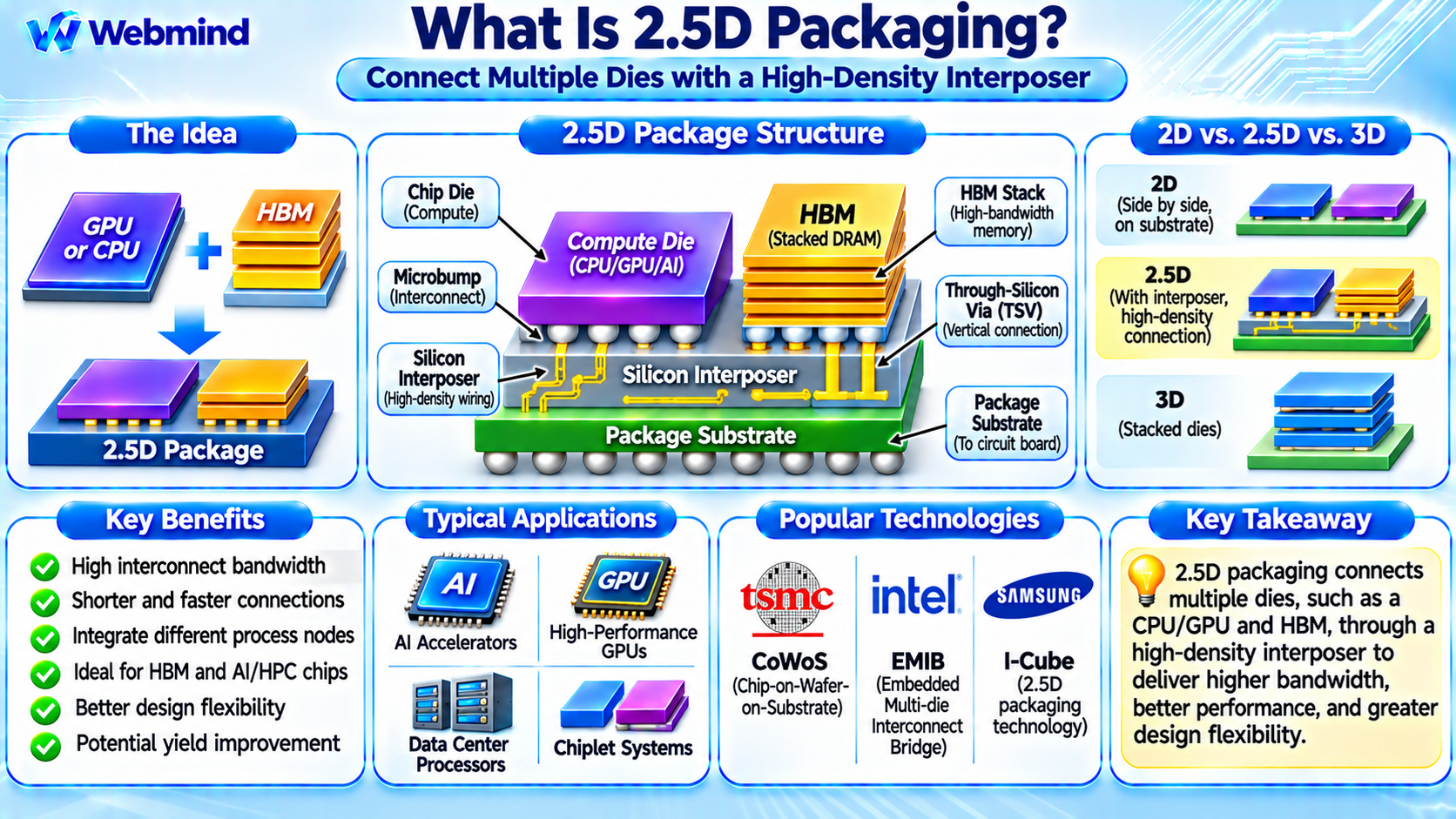
2.5D packaging is an advanced semiconductor packaging technology that connects multiple semiconductor dies within a single package using high-density interconnections.
It is widely used in high-performance computing, artificial intelligence accelerators, GPUs, and advanced memory systems.
Unlike traditional monolithic chips, where most computing functions are integrated onto one silicon die, 2.5D packaging allows separate dies to communicate through a shared interposer or other high-density interconnect structures.
For example, an AI accelerator can place a GPU die next to several High Bandwidth Memory (HBM) stacks, connecting them through a silicon interposer.
This architecture provides high communication bandwidth while allowing different components to be manufactured separately.
How Does 2.5D Packaging Work?
In a typical 2.5D package, multiple semiconductor dies are mounted side by side on an interposer.
The interposer contains extremely fine electrical connections that allow signals to travel between the dies.
The interposer is then connected to a larger package substrate, which provides electrical connections to the system board.
For example, a GPU and several HBM stacks may be connected through thousands of short interconnects.
This provides much wider memory interfaces than conventional board-level memory connections.
Although the components are physically separate dies, they can function together as a highly integrated computing system.
Not all 2.5D packages use a full silicon interposer. Some use silicon bridges or other high-density packaging structures.
Main Components of a 2.5D Package
A modern 2.5D semiconductor package commonly contains several important components.
Compute Die: A semiconductor die containing processing circuits such as CPU cores, GPU execution units, or AI accelerators.
Memory Dies: Separate semiconductor devices, often arranged in HBM stacks, that provide high-bandwidth data storage.
Interposer: A high-density interconnection structure that connects neighboring dies.
Microbumps: Tiny conductive connections between semiconductor dies and the interposer or bridge structures.
Package Substrate: Provides mechanical support and routes power and signals between the package and the external circuit board.
Through-Silicon Vias (TSVs): Vertical electrical connections used in certain silicon interposers and stacked memory devices.
Thermal Interface and Cooling Structures: Help transfer heat away from the active semiconductor components.
The exact arrangement depends on the packaging technology and chip architecture.
What Is a Silicon Interposer?
A silicon interposer is a thin piece of silicon containing fine-pitch metal interconnections.
Unlike an ordinary processor die, a passive silicon interposer generally does not contain the main computing circuitry. Its primary purpose is to provide dense electrical connections between neighboring dies.
Silicon interposers can support much finer wiring than typical organic package substrates.
This allows thousands of signals to connect nearby chips through short electrical paths.
Some interposers also contain Through-Silicon Vias that connect the upper interconnection layers to the package substrate below.
The interposer is one of the key technologies enabling high-bandwidth communication in many advanced 2.5D packages.
2D vs. 2.5D vs. 3D Packaging
Semiconductor packaging can be classified according to how multiple dies are physically arranged and interconnected.
2D Packaging
In conventional 2D multi-die packaging, semiconductor dies are placed side by side on a package substrate.
Electrical connections are routed primarily through the substrate.
This approach is suitable for many applications but may provide lower interconnection density than more advanced packaging methods.
2.5D Packaging
In 2.5D packaging, multiple dies are placed side by side and connected through a high-density interposer or bridge.
This supports shorter connections and greater interconnect density.
3D Packaging
In 3D packaging, semiconductor dies are stacked vertically.
Electrical connections may use TSVs, hybrid bonding, or other vertical interconnect technologies.
Three-dimensional integration can provide extremely dense connections but introduces additional thermal and manufacturing challenges.
These technologies are not mutually exclusive. A 2.5D package may contain vertically stacked HBM devices, combining different forms of integration.
Why Is 2.5D Packaging Important for HBM?
High Bandwidth Memory is one of the most important applications of 2.5D packaging.
HBM uses vertically stacked DRAM dies connected through TSVs.
Unlike conventional DDR memory modules, HBM uses a very wide memory interface and relatively short electrical connections to communicate with processing hardware.
A 2.5D package can place multiple HBM stacks next to a GPU or AI accelerator.
The interposer provides high-density connections between the processor and memory stacks.
This architecture can deliver extremely high aggregate memory bandwidth while reducing the energy required for certain data transfers compared with longer, narrower interfaces.
HBM is particularly valuable for AI training, AI inference, scientific computing, and other memory-bandwidth-intensive workloads.
2.5D Packaging and Chiplet Technology
Chiplets are small semiconductor dies designed to operate together within a larger computing system.
2.5D packaging provides one way to connect chiplets through high-density interconnections.
For example, a package may contain separate CPU, GPU, AI accelerator, and I/O chiplets.
These dies can communicate through an interposer or bridge structure.
One important advantage is that different chiplets may use different manufacturing process nodes.
A compute die may use an advanced logic process, while an I/O die uses a more mature and cost-effective technology.
This flexibility can improve manufacturing economics and allow chip designers to optimize each component separately.
However, chiplet integration also requires careful coordination of electrical interfaces, power delivery, signal timing, and thermal management.
Common 2.5D Packaging Technologies
Several semiconductor manufacturers and packaging providers have developed advanced 2.5D integration technologies.
TSMC CoWoS (Chip-on-Wafer-on-Substrate): A family of advanced packaging technologies used to integrate computing dies and HBM. Different CoWoS variants use different interposer or redistribution structures.
Intel EMIB (Embedded Multi-die Interconnect Bridge): Uses small silicon bridge structures embedded in a package substrate to provide high-density connections between neighboring dies.
Samsung I-Cube: A 2.5D integration technology designed to connect logic dies and HBM using interposer-based packaging approaches.
These technologies differ in physical structure, manufacturing methods, cost, and interconnection capabilities.
The choice depends on chip size, interconnect bandwidth, memory requirements, and packaging economics.
Advantages of 2.5D Packaging
High Interconnect Bandwidth: Fine-pitch connections allow large amounts of data to move between nearby dies.
Shorter Electrical Paths: Short connections can reduce certain signal losses and communication energy costs.
Heterogeneous Integration: Different semiconductor functions and manufacturing processes can be combined in one package.
Improved Design Flexibility: Manufacturers can develop and test individual dies before package assembly.
Support for HBM: Enables high-bandwidth connections between compute dies and stacked memory.
Potential Yield Benefits: Smaller dies can improve wafer-level yield compared with some large monolithic designs.
These advantages make 2.5D packaging attractive for advanced computing systems.
Challenges of 2.5D Packaging
Despite its benefits, 2.5D packaging introduces several technical difficulties.
Manufacturing Cost: Silicon interposers, microbumps, advanced substrates, and assembly equipment increase production expenses.
Interposer Size: Large computing systems may require interconnection structures that exceed conventional manufacturing dimensions.
Thermal Management: Multiple high-power dies and HBM stacks generate heat within a limited package area.
Power Delivery: Advanced processors require stable electrical power distributed across multiple dies.
Assembly Yield: Defects in bonding or interconnections can cause the complete package to fail.
Mechanical Reliability: Different materials expand and contract differently during temperature changes.
These challenges require precise manufacturing, testing, and thermal engineering.
Where Is 2.5D Packaging Used?
2.5D packaging is particularly important in high-performance semiconductor products.
AI Accelerators: Connect compute dies with multiple HBM stacks for neural network processing.
High-Performance GPUs: Support high-bandwidth memory connections for scientific computing and advanced graphics workloads.
Data Center Processors: Enable integration of multiple compute and I/O dies.
Networking ASICs: Support high-speed communication and specialized packet-processing hardware.
High-Performance Computing (HPC): Provides the memory bandwidth and interconnect density required by large scientific workloads.
Advanced Chiplet Systems: Connect specialized dies within one semiconductor package.
The technology is especially valuable when communication bandwidth between dies becomes a major performance requirement.
The Future of 2.5D Packaging
As transistor scaling becomes more expensive, advanced packaging is playing a larger role in semiconductor development.
Future processors may combine multiple compute chiplets, specialized accelerators, and increasingly large HBM configurations.
Manufacturers are also developing larger interposer structures, improved silicon bridges, advanced redistribution layers, and finer-pitch bonding technologies.
These improvements can increase the number of connected dies and the available communication bandwidth.
At the same time, 2.5D packaging will continue to coexist with conventional 2D packaging and vertically stacked 3D integration.
The most suitable technology depends on performance requirements, power consumption, manufacturing cost, and system complexity.
Conclusion
2.5D packaging is an advanced semiconductor integration technology that connects multiple dies side by side through high-density interposers or bridge structures.
It enables fast communication between processors, chiplets, and High Bandwidth Memory while allowing different semiconductor components to be manufactured separately.
Technologies such as CoWoS, EMIB, and I-Cube demonstrate how advanced packaging can support complex multi-die computing systems.
Although 2.5D packaging introduces challenges involving cost, heat, power delivery, and manufacturing complexity, it has become an essential technology for modern AI accelerators, high-performance GPUs, and data center computing.
Understanding 2.5D packaging provides an important foundation for studying chiplets, HBM, semiconductor interposers, 3D integration, advanced processor architecture, and modern semiconductor manufacturing.