Introduction
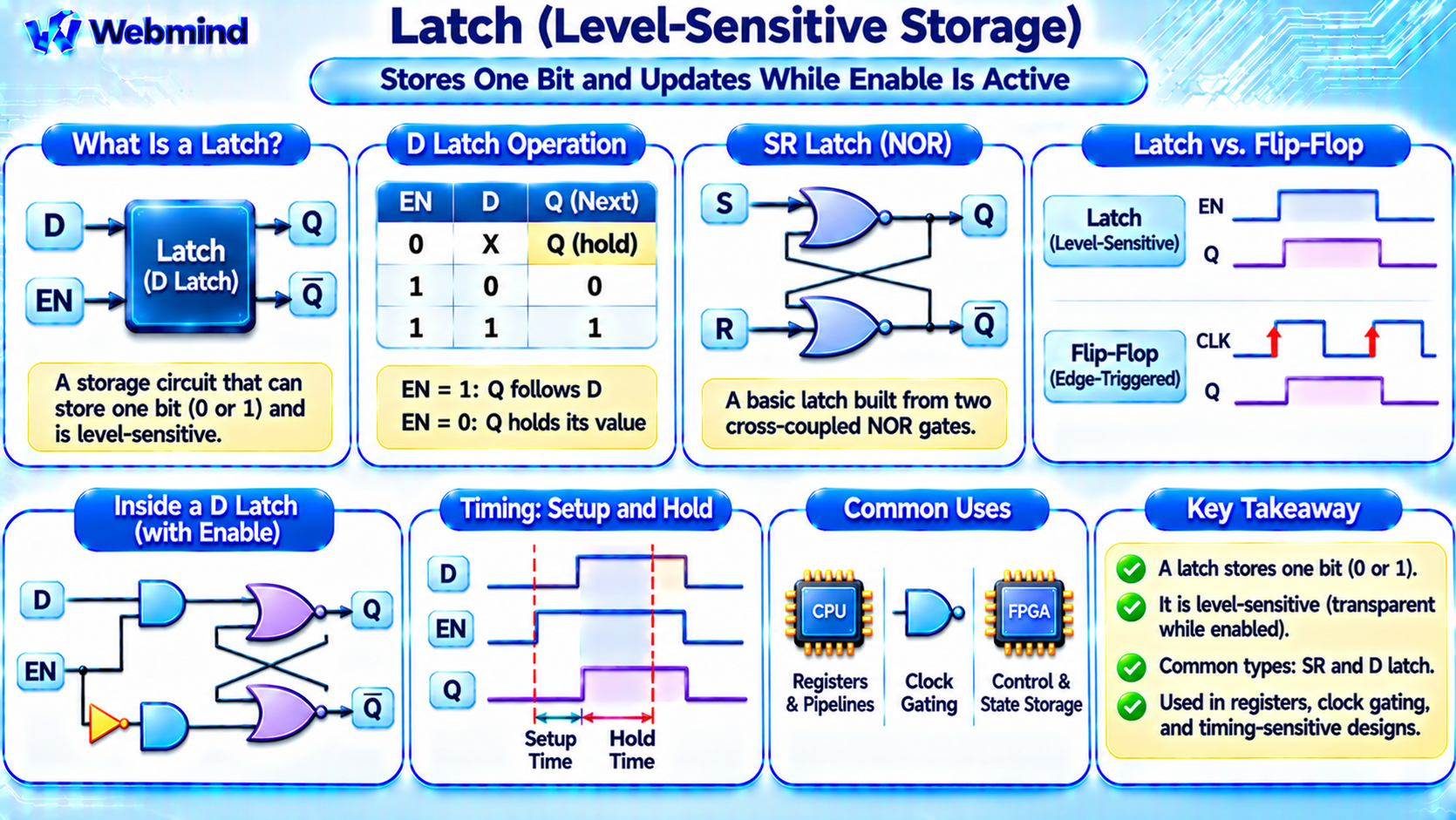
A latch is a digital electronic circuit that stores one bit of binary information, either 0 or 1.
It is a fundamental building block of sequential logic and is used in digital systems that need to retain information.
Unlike a combinational logic circuit, whose output depends only on current inputs, a latch can remember its previous state.
This makes it useful for temporary data storage, control circuits, and timing-related applications.
Latches are closely related to flip-flops, but an important difference is that a typical latch is level-sensitive, while a flip-flop is edge-triggered.
Understanding latches is essential for studying registers, memory circuits, CPU architecture, FPGA design, and digital electronics.
How Does a Latch Work?
A latch stores information using a feedback circuit that can maintain one of two stable logical states.
Its main output is commonly labeled Q. Some latches also provide a complementary output, labeled Q’.
A latch changes its stored value according to its input and control signals.
For example, a D latch has a data input D and an enable input EN.
When the enable signal is active, the output follows the data input after a short propagation delay.
When the enable signal becomes inactive, the latch retains the last stored value.
This behavior is called level-sensitive storage.
Because the latch can remember its previous state, it belongs to the category of sequential logic circuits.
What Is an SR Latch?
An SR latch, also called a Set-Reset latch, is one of the simplest storage circuits.
It can be constructed using two cross-coupled NOR gates or two cross-coupled NAND gates.
The cross-coupled connections provide feedback, allowing the circuit to maintain its state.
For a conventional active-high NOR-based SR latch, the behavior is:
S = 0, R = 0: Hold the previous state.
S = 1, R = 0: Set Q to 1.
S = 0, R = 1: Reset Q to 0.
S = 1, R = 1: Forbidden or invalid operating condition.
The invalid condition occurs because both outputs are forced to the same logical level, violating their intended complementary relationship.
An SR latch demonstrates how feedback can create a circuit capable of storing information.
What Is a D Latch?
A D latch, or Data latch, is a level-sensitive storage element that typically has three main signals: D, Enable, and Q.
The D input provides the data to be stored.
The Enable input determines whether the latch can update its stored value.
For an active-high D latch:
EN = 1: Q follows D.
EN = 0: Q retains its previous value.
For example, if EN = 1 and D changes from 0 to 1, Q also changes to 1 after the circuit’s propagation delay.
When EN becomes 0, the latch stores the last value of D.
Even if D changes afterward, Q remains unchanged until the latch is enabled again.
D latches are widely used because they provide controlled storage without the invalid input combination found in a basic SR latch.
What Does Transparent Mean in a Latch?
A latch is called transparent when its output can follow changes at its data input.
For an active-high D latch, transparency occurs while Enable = 1.
During this period, a change at D can propagate through the latch to Q.
When Enable changes to 0, the latch stops following the input and retains the stored value.
This behavior differs from an edge-triggered flip-flop, which normally updates only at a specific clock transition.
Transparency can be useful in timing-sensitive designs, but it also requires careful control.
If a signal passes through several transparent latches simultaneously, unexpected timing behavior or race conditions may occur.
Latch vs. Flip-Flop: What Is the Difference?
Latches and flip-flops both store one bit of binary information, but their timing behavior is different.
Latch: Usually level-sensitive. It can update continuously while its enable or clock-control level is active.
Flip-Flop: Usually edge-triggered. It captures the input value at a rising or falling clock edge.
For example, an active-high D latch follows the D input while Enable = 1.
A positive-edge-triggered D flip-flop captures D only when the clock changes from low to high.
Flip-flops are widely used in conventional synchronous register-based designs because their edge-triggered behavior simplifies many timing relationships.
Latches remain important in selected high-performance, low-power, and specialized circuit designs.
How Is a Latch Built from Logic Gates?
A basic SR latch can be constructed using two NOR gates connected in a feedback arrangement.
The output of each NOR gate connects to an input of the other NOR gate.
This feedback allows the circuit to maintain a stable state after the Set or Reset input returns to its inactive value.
A NAND-based SR latch uses a similar arrangement but normally has active-low Set and Reset inputs.
A D latch can be constructed by adding control logic that generates appropriate Set and Reset signals from the D and Enable inputs.
Modern integrated circuits may instead use optimized transistor-level latch structures.
The exact implementation depends on power consumption, timing requirements, transistor count, and manufacturing technology.
What Is a Gated Latch?
A gated latch includes a control signal that determines when the storage element is allowed to update.
For example, a gated SR latch adds an Enable input to the basic SR storage structure.
When Enable is inactive, the latch retains its previous value.
When Enable is active, the Set and Reset inputs can control the stored state.
A D latch is another form of gated storage circuit because its Enable input determines when data can pass into the storage element.
Gated latches are useful when a digital system needs controlled data storage rather than continuous changes.
How Are Latches Used in Registers?
A register is a collection of storage elements used to hold multiple bits of data.
For example, an eight-bit register requires storage for eight binary bits.
Registers can be constructed using latches or flip-flops, depending on the required timing architecture.
A latch-based register can update while its enable signal is active and hold its data when the enable becomes inactive.
In contrast, a conventional flip-flop-based register captures data at a clock edge.
Latch-based designs can support timing techniques such as time borrowing, but they require more complex timing analysis.
What Is Time Borrowing?
Time borrowing is an important concept in latch-based digital circuit design.
In an edge-triggered system, data generally must arrive before a specific clock edge to satisfy setup timing requirements.
In a latch-based system, a transparent latch may continue accepting data during part of its active clock phase.
This allows a combinational logic path to use some time that would otherwise belong to the following stage.
The technique can help balance delays between pipeline stages and improve timing flexibility.
However, time borrowing requires careful clock-phase design, hold-time analysis, and control of race conditions.
It is therefore more complex than conventional edge-triggered timing.
What Are Setup Time and Hold Time?
Latches have timing requirements similar to other sequential storage elements.
Setup Time: Data must remain stable for a specified interval before the latch closes and stops accepting new data.
Hold Time: Data must remain stable for a specified interval after the latch closes.
Violating these timing constraints can cause incorrect data capture or metastability.
Metastability is a condition in which a storage element temporarily fails to resolve quickly to a stable logical state.
Latch-based designs also require analysis of transparency windows and the possibility of data propagating through multiple storage stages.
Static Timing Analysis (STA) tools help engineers verify these requirements.
Latches in CPUs and ASICs
Latches are used in various semiconductor circuits, including selected high-performance processor designs.
They may appear in timing-sensitive pipelines, control structures, and internal storage circuits.
Processor Pipelines: Latch-based stages can support time borrowing and flexible timing optimization.
Control Circuits: Latches can retain control states or enable signals.
ASIC Designs: Standard-cell libraries may provide latch cells optimized for area, timing, or power.
Clock-Gating Circuits: Latches are often used to hold clock-enable signals stable and prevent unwanted glitches.
Although many synchronous systems rely heavily on flip-flops, latches remain valuable when their timing characteristics offer specific advantages.
Latches in FPGAs
Modern FPGAs primarily provide dedicated flip-flop resources for synchronous data storage.
However, latch behavior can still be described using Verilog or VHDL.
Whether a latch can be implemented efficiently depends on the FPGA architecture and synthesis tool.
In many FPGA designs, unintended latch inference is considered undesirable because it can complicate timing analysis and produce unexpected behavior.
For example, an incomplete assignment in a combinational Verilog block may cause synthesis software to infer a latch.
FPGA designers generally avoid accidental latches by ensuring that combinational outputs are assigned in every required execution path.
Intentional latch designs should be used only when the hardware architecture and timing requirements support them.
How Is a Latch Described in Verilog?
A D latch can be described in Verilog using a level-sensitive process.
For example, in SystemVerilog:
always_latch if (en) q <= d;
This describes a latch that follows D while Enable is active and retains its value otherwise.
The always_latch construct explicitly communicates the designer’s intention to create latch behavior.
In contrast, a flip-flop is normally described using an edge-sensitive process such as always_ff @(posedge clk).
Modern EDA tools can identify inferred latches and report warnings when latch behavior appears unexpectedly.
Understanding this distinction is important when writing synthesizable hardware descriptions.
Why Can Accidental Latches Be a Problem?
An accidental latch occurs when hardware description code unintentionally requires a signal to retain its previous value.
For example, a combinational process that assigns an output only when a condition is true may leave the output unchanged when the condition is false.
To preserve that previous value, synthesis software may infer a latch.
This can create unexpected timing behavior and complicate circuit verification.
Accidental latches may also introduce transparency-related timing paths that were not considered in the original design.
To avoid this problem, engineers typically assign default values and ensure all outputs are assigned in every branch of intended combinational logic.
Advantages of Latches
Simple Storage: A latch can store one bit using a relatively compact circuit.
Level-Sensitive Operation: Data can be captured during an enable interval rather than only at a clock edge.
Time Borrowing: Latch-based pipelines can redistribute timing margins between stages.
Potential Area Efficiency: Some latch implementations require fewer transistors than comparable flip-flop structures.
Clock-Gating Applications: Latches help create stable enable signals in glitch-free clock-gating circuits.
These benefits make latches useful in specialized digital system designs.
Limitations of Latches
Latches also introduce important design challenges.
Timing Complexity: Transparent operation requires careful analysis of signal propagation and clock phases.
Race Conditions: Data may propagate through multiple enabled latch stages unexpectedly.
Hold-Time Sensitivity: Latch-based systems can require strict hold-time control.
Accidental Inference: Incomplete hardware description code can unintentionally create latch behavior.
FPGA Compatibility: Dedicated latch resources are less common than flip-flop resources in many FPGA architectures.
These limitations explain why edge-triggered flip-flops are often preferred in introductory synchronous digital designs.
Where Are Latches Used?
Latches are used in several areas of digital electronics.
CPUs: Selected pipeline structures, control circuits, and timing-sensitive storage applications.
ASICs: Custom sequential logic and optimized standard-cell implementations.
Clock-Gating Circuits: Hold enable signals stable to avoid unwanted clock pulses.
Digital Controllers: Retain temporary control information.
Register Structures: Provide level-sensitive data storage in suitable circuit architectures.
Embedded Hardware: Implement selected state-holding and control functions.
Their role is particularly important in understanding sequential logic and circuit timing.
Conclusion
A latch is a level-sensitive sequential logic circuit that stores one bit of binary information.
Common types include SR latches, D latches, and gated latches.
Unlike an edge-triggered flip-flop, a latch can follow its data input while its enable signal is active and retain the stored value when the enable becomes inactive.
Latches are important in digital storage, clock-gating circuits, timing-sensitive pipelines, and specialized ASIC implementations.
Understanding latches provides an essential foundation for studying flip-flops, registers, clock signals, setup and hold timing, Verilog, FPGA development, and digital circuit design.