Introduction
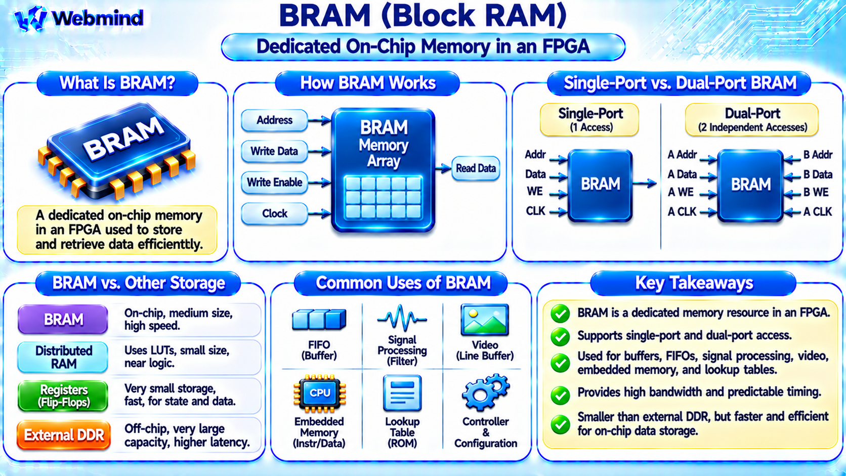
BRAM, or Block Random Access Memory, is a dedicated on-chip memory resource found in Field-Programmable Gate Arrays (FPGAs).
It allows FPGA designs to store and access data without relying entirely on external memory devices or general-purpose logic resources.
BRAM is widely used for data buffers, First-In-First-Out (FIFO) queues, lookup tables, temporary storage, and digital signal processing applications.
Unlike FPGA Look-Up Tables (LUTs), which primarily implement combinational logic, BRAM provides larger memory arrays designed for efficient data storage and retrieval.
Understanding BRAM is important for learning FPGA architecture, memory systems, Verilog, and digital hardware design.
How Does BRAM Work?
BRAM consists of dedicated memory blocks manufactured directly into an FPGA.
Each block contains a fixed amount of physical storage, but the available memory can often be configured with different data widths and depths.
For example, a memory block may be configured to store many narrow data words or fewer wide data words.
An FPGA circuit accesses BRAM using address, data, and control signals.
During a write operation, the circuit provides an address, input data, and a write-enable signal. The memory stores the data at the selected address, typically on a clock edge.
During a read operation, the circuit supplies an address and receives the stored data according to the memory block’s configured timing behavior.
Many FPGA BRAM implementations support synchronous read operations, in which output data becomes available after a clock edge.
Main Components of BRAM
A typical BRAM block contains several important elements.
Memory Array: Stores binary information in dedicated semiconductor memory cells.
Address Inputs: Select the memory location to be accessed.
Data Inputs: Carry information that will be written into memory.
Data Outputs: Provide information read from the selected memory location.
Clock Input: Coordinates memory operations in synchronous BRAM implementations.
Write Enable: Controls whether incoming data is stored at the selected address.
Read Enable or Output Enable: Controls reading or output behavior, depending on the FPGA architecture.
Optional Output Registers: Can improve timing performance by registering memory output data.
The exact signals and capabilities depend on the FPGA manufacturer and device family.
What Is BRAM Capacity?
BRAM capacity is commonly measured in kilobits.
For example, some AMD FPGA architectures provide dedicated memory blocks with capacities of 18 Kb or 36 Kb.
A 36 Kb block contains 36,864 bits when Kb represents 1,024 bits.
The memory can be configured into different width and depth arrangements supported by the hardware.
For example, ignoring architecture-specific restrictions and parity configurations, 36,864 bits could theoretically hold 4,096 words of 9 bits each.
Other FPGA families use different memory block sizes and organizations.
An FPGA may contain hundreds or thousands of dedicated memory blocks, depending on the device.
The total available BRAM capacity is therefore an important specification when selecting an FPGA for a particular application.
What Is Single-Port BRAM?
Single-port BRAM provides one memory access port.
A port generally contains address, data, and control signals that allow reading or writing memory locations.
For example, a single-port memory may perform a read operation during one clock cycle and a write operation during another.
The exact capabilities depend on the block’s configuration.
Single-port BRAM is suitable for many applications that require straightforward data storage and access.
Examples include small buffers, coefficient storage, and temporary data arrays.
What Is Dual-Port BRAM?
Many FPGA BRAM blocks support dual-port operation.
A dual-port memory provides two access interfaces that can operate independently within the capabilities of the hardware.
For example, one port may write incoming data while another port reads previously stored data.
This is useful for data buffering and communication between processing stages.
Some FPGA architectures support true dual-port memory, allowing both ports to perform reads or writes.
Other configurations provide one dedicated write port and one read port, often called simple dual-port memory.
Simultaneous access to the same address may have restrictions or device-specific behavior.
Designers must consult the target FPGA’s memory documentation to understand these conditions.
What Is BRAM Read Latency?
Read latency describes the time between requesting memory data and receiving the corresponding output.
In many FPGA BRAM configurations, the read operation is synchronous.
An address is presented before a clock edge, and the corresponding data becomes available after the edge, subject to the memory’s clock-to-output delay.
If additional output registers are enabled, the observable latency may increase by one or more clock cycles.
This behavior is important when designing high-speed FPGA pipelines.
For example, a processing circuit must account for BRAM latency when coordinating address generation, data processing, and output timing.
BRAM is generally optimized for predictable, high-speed access within FPGA hardware.
What Happens During Simultaneous Read and Write?
A BRAM block may receive read and write requests involving the same memory address.
The resulting behavior depends on the FPGA architecture and memory configuration.
Common read-during-write modes include:
Write-First: The output reflects the newly written data.
Read-First: The output reflects the previously stored data.
No-Change: The output retains its previous value during certain write operations.
These descriptions are simplified, and exact collision behavior varies between devices and port configurations.
Some simultaneous operations involving the same address may produce undefined or unsupported results.
FPGA designers should verify the supported modes when implementing dual-port memories.
BRAM vs. Distributed RAM
FPGAs commonly provide more than one type of on-chip memory.
BRAM: Uses dedicated memory blocks designed for relatively large storage arrays.
Distributed RAM: Uses memory-capable LUT resources to implement smaller writable memory structures.
BRAM is generally suitable for larger buffers and memory arrays.
Distributed RAM can be useful for small memories located close to logic circuits.
However, distributed RAM consumes LUT resources that might otherwise implement combinational logic.
The choice depends on memory size, access requirements, timing, and resource availability.
EDA synthesis tools may automatically select an appropriate memory implementation based on the HDL description and target FPGA.
BRAM vs. Registers
BRAM and flip-flop registers both store binary information, but their hardware structures and intended uses differ.
Registers are particularly useful for storing small amounts of data that must be accessed directly by logic.
For example, an eight-bit register can be implemented using eight flip-flops.
BRAM provides a denser memory structure for storing larger amounts of information.
A register-based memory with thousands of bits may consume substantial FPGA logic resources.
Using BRAM can preserve those resources for other digital functions.
However, registers may provide more flexible access patterns or lower latency for certain small storage structures.
BRAM vs. External DDR Memory
BRAM is located inside the FPGA chip, while DDR memory is typically implemented using external DRAM devices.
BRAM: Provides relatively small storage capacity with predictable access timing and high internal bandwidth.
DDR Memory: Provides much greater capacity but requires a memory controller and external memory interface.
For example, an FPGA may use BRAM to buffer incoming data while DDR stores a much larger dataset.
BRAM can also serve as temporary working memory for processing pipelines.
External DDR is useful when the application requires storage capacities beyond the FPGA’s on-chip memory resources.
Many high-performance FPGA systems combine BRAM with external DDR, HBM, or other memory technologies.
How Is BRAM Used in FIFO Buffers?
A FIFO, or First-In-First-Out buffer, stores data in the order it arrives.
The first item written into the buffer is the first item read out.
BRAM is commonly used to implement FIFOs because it provides efficient storage for sequential data.
A typical FIFO includes memory, read and write pointers, and control logic.
The write pointer identifies where new data will be stored, while the read pointer identifies the next data item to retrieve.
Additional logic determines whether the FIFO is empty or full.
FIFOs are widely used in FPGA communication interfaces, streaming pipelines, and data acquisition systems.
Some FIFOs also support separate read and write clock domains, requiring specialized clock-domain crossing techniques.
BRAM in Digital Signal Processing
Digital signal processing applications often require temporary storage for samples and coefficients.
For example, a Finite Impulse Response (FIR) filter processes a sequence of input samples using mathematical coefficients.
BRAM can store input samples, delay-line data, or filter coefficients.
DSP blocks perform arithmetic operations such as multiplication and accumulation.
LUTs and registers provide control and pipeline logic.
By combining BRAM, DSP blocks, and programmable logic, an FPGA can implement efficient real-time signal-processing systems.
This architecture is useful in communications, audio processing, image processing, and sensor applications.
BRAM in FPGA State Machines and Controllers
BRAM can also support control-oriented digital circuits.
A finite state machine usually stores its current state in registers and implements transition logic using LUTs.
However, more complex controllers may use BRAM to store instruction sequences, microcode, configuration data, or lookup information.
For example, a custom hardware controller can read predefined control words from BRAM.
The selected control word may determine which operations are performed during the next processing step.
This approach can reduce some combinational logic complexity when the controller requires a large set of predefined output patterns.
How Is BRAM Described in Verilog?
FPGA developers can describe memory arrays using Verilog or SystemVerilog.
For example, a memory declaration may be written as:
reg [7:0] mem [0:1023];
This describes 1,024 memory locations, each containing eight bits.
The total storage capacity is 8,192 bits.
A clocked process can write data into the memory when a write-enable signal is active.
A synchronous read process can retrieve data from the selected address.
During synthesis, the FPGA development tool may infer BRAM if the memory description matches a supported hardware structure.
However, BRAM inference is not guaranteed by the declaration alone.
Read timing, write behavior, reset logic, port configuration, and synthesis settings can affect the implementation.
For more precise control, designers may instantiate vendor-provided BRAM primitives or memory IP blocks.
What Is BRAM Initialization?
Some FPGA architectures allow BRAM contents to be initialized when the device is configured.
For example, a memory block may contain predefined lookup values, filter coefficients, or processor program data.
The initialization information can be included in the FPGA configuration bitstream.
During device configuration, the memory receives its initial contents.
After configuration, the stored data can generally be read or modified during normal operation, depending on the memory configuration.
This makes BRAM useful for implementing small ROM-like memories as well as writable RAM.
However, ordinary SRAM-based BRAM is volatile and loses its stored information when power is removed.
How Does BRAM Affect FPGA Performance?
BRAM provides dedicated memory resources that can improve FPGA implementation efficiency.
Important characteristics include storage capacity, memory width, operating frequency, read latency, and port configuration.
A well-designed FPGA pipeline can use multiple BRAM blocks in parallel to supply substantial data bandwidth.
However, BRAM access is still subject to physical limitations.
A single memory port cannot provide an unlimited number of independent accesses in one cycle.
Applications requiring multiple simultaneous reads or writes may need memory replication, banking, or other architectural techniques.
FPGA designers must balance memory bandwidth, storage capacity, logic utilization, and timing requirements.
Applications of BRAM
BRAM is widely used in FPGA-based systems.
Data Buffers: Temporarily store incoming or outgoing information.
FIFO Queues: Support streaming data and communication interfaces.
Digital Signal Processing: Store samples, coefficients, and intermediate results.
Video Processing: Implement line buffers and temporary pixel storage.
Embedded Processors: Provide instruction memory, data memory, and small local storage structures.
Lookup Tables: Store predefined numerical values or control information.
Communication Systems: Buffer network packets and protocol data.
Control Systems: Store configuration information and predefined operation sequences.
These applications demonstrate why dedicated memory blocks are essential in modern FPGA architectures.
Advantages of BRAM
Efficient Storage Density: Dedicated memory blocks store substantial data without consuming large numbers of general-purpose logic cells.
High On-Chip Bandwidth: Multiple BRAM blocks can provide parallel access to data.
Predictable Timing: Synchronous memory operations can be integrated into carefully controlled FPGA pipelines.
Configurable Organization: Many devices support different memory widths, depths, and port arrangements.
Logic Resource Savings: Using BRAM preserves LUTs and registers for other circuit functions.
Flexible Applications: BRAM can implement RAM, ROM-like storage, FIFOs, and specialized buffers.
Limitations of BRAM
BRAM also has several limitations.
Limited Capacity: On-chip BRAM provides much less storage than large external DRAM systems.
Fixed Physical Blocks: Memory allocation may waste capacity when a design does not fit the supported block configurations efficiently.
Port Restrictions: The number of simultaneous memory accesses is limited.
Read Latency: Synchronous operations introduce clock-dependent access timing.
Collision Behavior: Simultaneous access to the same address may require special handling.
Volatility: SRAM-based BRAM generally loses its data when the device is powered off.
These limitations influence how FPGA memory systems are designed.
Conclusion
BRAM, or Block Random Access Memory, is a dedicated on-chip memory resource used in FPGAs to store and retrieve binary data efficiently.
It supports applications such as FIFOs, data buffers, lookup tables, embedded processor memories, and digital signal-processing pipelines.
Compared with LUT-based distributed RAM and flip-flop registers, BRAM provides denser storage for larger memory arrays.
Modern FPGA systems combine BRAM with LUTs, registers, DSP blocks, programmable routing, and external memory to implement complex digital hardware.
Understanding BRAM is essential for studying FPGA architecture, Verilog memory inference, FIFO design, digital signal processing, and embedded hardware development.