Introduction
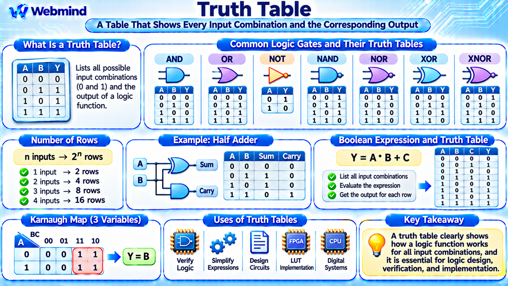
A truth table is a mathematical tool that shows every possible combination of inputs to a logic function and the corresponding output.
It is widely used in Boolean algebra, digital electronics, computer architecture, and logic circuit design.
Truth tables provide a clear way to describe how logic gates such as AND, OR, NOT, XOR, NAND, and NOR operate.
They are also essential for designing more complex circuits, including adders, multiplexers, decoders, and digital control systems.
In FPGA and ASIC development, truth tables help engineers understand, verify, and implement logical functions before building hardware.
How Does a Truth Table Work?
A truth table lists all possible binary input combinations and calculates the output for each combination.
Digital logic uses two logical values: 0 and 1, commonly representing false and true.
For example, a circuit with two inputs, A and B, has four possible combinations:
A = 0, B = 0
A = 0, B = 1
A = 1, B = 0
A = 1, B = 1
A truth table adds an output column, usually labeled Y, showing the result of the logical operation for each combination.
A circuit with n binary inputs has 2ⁿ possible input combinations.
Therefore, two inputs produce four rows, three inputs produce eight rows, and four inputs produce sixteen rows.
Truth Table for an AND Gate
An AND gate produces a logical 1 only when all its inputs are 1.
Its Boolean expression is:
Y = A AND B
The truth table is:
A = 0, B = 0 → Y = 0
A = 0, B = 1 → Y = 0
A = 1, B = 0 → Y = 0
A = 1, B = 1 → Y = 1
For example, an industrial control circuit might activate a machine only when the start button is pressed and a safety condition is satisfied.
The AND gate represents a situation where both conditions must be true.
Truth Table for an OR Gate
An OR gate produces 1 when at least one input is 1.
Its Boolean expression is:
Y = A OR B
The four combinations are:
A = 0, B = 0 → Y = 0
A = 0, B = 1 → Y = 1
A = 1, B = 0 → Y = 1
A = 1, B = 1 → Y = 1
An OR gate can combine multiple conditions.
For example, an alarm system may activate when either a temperature sensor or a pressure sensor detects an abnormal condition.
Truth Table for a NOT Gate
A NOT gate, also called an inverter, has one input and one output.
It reverses the logical value of its input.
Y = NOT A
Its truth table contains only two combinations:
A = 0 → Y = 1
A = 1 → Y = 0
A NOT gate is one of the simplest digital logic circuits.
A basic CMOS inverter uses one PMOS transistor and one NMOS transistor to implement this operation.
Truth Tables for NAND and NOR Gates
NAND and NOR gates are combinations of basic logical operations.
NAND Gate
A NAND gate performs an AND operation followed by inversion.
Y = NOT (A AND B)
A = 0, B = 0 → Y = 1
A = 0, B = 1 → Y = 1
A = 1, B = 0 → Y = 1
A = 1, B = 1 → Y = 0
NOR Gate
A NOR gate performs an OR operation followed by inversion.
Y = NOT (A OR B)
A = 0, B = 0 → Y = 1
A = 0, B = 1 → Y = 0
A = 1, B = 0 → Y = 0
A = 1, B = 1 → Y = 0
NAND and NOR are called universal gates because any Boolean function can be constructed using only NAND gates or only NOR gates.
Truth Tables for XOR and XNOR Gates
XOR and XNOR gates are commonly used in arithmetic and comparison circuits.
XOR Gate
XOR stands for Exclusive OR.
It produces 1 when its two inputs are different.
Y = A XOR B
A = 0, B = 0 → Y = 0
A = 0, B = 1 → Y = 1
A = 1, B = 0 → Y = 1
A = 1, B = 1 → Y = 0
XNOR Gate
XNOR produces 1 when its two inputs are equal.
Y = NOT (A XOR B)
A = 0, B = 0 → Y = 1
A = 0, B = 1 → Y = 0
A = 1, B = 0 → Y = 0
A = 1, B = 1 → Y = 1
XOR is useful for binary addition, while XNOR is commonly used in equality comparison circuits.
How to Create a Truth Table
Creating a truth table follows a systematic process.
Step 1: Identify the Inputs. Determine the number of Boolean variables used by the logic function.
Step 2: Calculate the Number of Rows. Use 2ⁿ, where n is the number of inputs.
Step 3: List Input Combinations. Write every possible combination of zeros and ones.
Step 4: Evaluate the Expression. Calculate the logical result for each input combination.
Step 5: Record the Outputs. Add the results to the output column.
For example, consider:
Y = (A AND B) OR C
This function has three inputs, so its truth table contains eight rows.
The output becomes 1 whenever C = 1 or both A and B are 1.
This method works for any combinational Boolean function.
Truth Tables and Boolean Algebra
Truth tables and Boolean algebra describe the same logical behavior in different forms.
A truth table lists the results for every input combination.
A Boolean expression represents the function using mathematical operators.
For example:
Y = A AND B
describes the same function as the two-input AND truth table.
Different Boolean expressions can produce identical truth tables.
For example:
Y = A AND (B OR NOT B)
Since B OR NOT B always equals 1, the expression simplifies to:
Y = A
Both expressions produce the same output for every possible input combination.
Truth tables can therefore be used to verify whether two Boolean expressions are logically equivalent.
How Are Truth Tables Used in Binary Adders?
A half adder is a digital circuit that adds two binary digits.
It has two inputs, A and B, and two outputs: Sum and Carry.
The truth table is:
A = 0, B = 0 → Sum = 0, Carry = 0
A = 0, B = 1 → Sum = 1, Carry = 0
A = 1, B = 0 → Sum = 1, Carry = 0
A = 1, B = 1 → Sum = 0, Carry = 1
The Boolean expressions are:
Sum = A XOR B
Carry = A AND B
This example demonstrates how a truth table can describe a circuit with multiple outputs.
Full adders extend this principle to include an incoming carry bit.
These arithmetic circuits are important components of the Arithmetic Logic Unit (ALU) inside a CPU.
What Is the Relationship Between Truth Tables and Karnaugh Maps?
A Karnaugh map, or K-map, is a graphical method for simplifying Boolean functions.
It uses the same input-output information as a truth table but arranges the combinations in a special grid.
Adjacent cells differ by only one input variable.
By grouping adjacent cells containing 1, engineers can identify simpler Boolean expressions.
For example, a four-input Boolean function has sixteen combinations, which can be represented in a four-by-four Karnaugh map.
Karnaugh maps are particularly useful for simplifying relatively small logic circuits.
For more complex designs, EDA tools use automated logic optimization techniques.
How Are Truth Tables Used in FPGAs?
Truth tables are especially important in FPGA architecture.
Modern FPGAs commonly use Look-Up Tables (LUTs) to implement combinational logic functions.
A LUT stores the output values corresponding to possible input combinations.
For example, a two-input AND gate has four truth-table outputs:
0, 0, 0, 1
A two-input LUT can store these four bits and select the appropriate output using inputs A and B.
The same LUT can be reconfigured to implement OR, XOR, NAND, NOR, or another two-input Boolean function.
A LUT with four independent inputs can represent a single-output Boolean function with sixteen possible input combinations.
This connection between truth tables and LUTs explains how programmable logic devices implement digital circuits.
Truth Tables in Verilog and Digital Design
Hardware Description Languages such as Verilog and VHDL allow engineers to describe logic functions in software-like text.
For example, a Verilog assignment can describe the Boolean expression:
Y = A AND B
During simulation, an EDA tool evaluates the circuit behavior for different input combinations.
The results can be compared with the expected truth table.
During synthesis, the tool converts the hardware description into an implementation using gates, standard cells, or FPGA resources.
Truth tables therefore provide a useful reference for designing and verifying digital hardware.
However, practical Verilog simulation can also represent unknown and high-impedance states, commonly written as X and Z. These are simulation values rather than additional physical Boolean digits.
Truth Tables vs. Timing Diagrams
Truth tables describe the logical relationship between inputs and outputs.
They do not normally describe how long a physical circuit takes to respond.
For example, an AND gate truth table shows that inputs A = 1 and B = 1 produce Y = 1.
However, a real gate has propagation delay, so the output does not change instantaneously when an input changes.
A timing diagram shows signals changing over time and can illustrate propagation delays, clock edges, and other timing behavior.
Truth tables are therefore primarily used for logical correctness, while timing diagrams help explain dynamic circuit behavior.
Both are important for digital circuit design.
Why Are Truth Tables Important?
Truth tables provide a precise and systematic method for describing digital logic.
They allow engineers to evaluate logic gates, verify Boolean expressions, compare circuit implementations, and identify design errors.
Truth tables are also used to develop arithmetic circuits, decoders, multiplexers, control logic, and combinational parts of state machines.
In FPGA development, they directly explain how LUTs implement Boolean functions.
In ASIC design, they help define and verify the behavior of logic circuits before manufacturing.
Understanding truth tables is therefore an essential foundation for studying digital hardware.
Conclusion
A truth table lists every possible combination of Boolean inputs and the corresponding output of a logic function.
It provides a clear description of how AND, OR, NOT, NAND, NOR, XOR, and XNOR gates operate.
Truth tables are also essential for Boolean algebra, logic simplification, binary arithmetic, circuit verification, and FPGA LUT implementation.
Although truth tables describe logical behavior rather than physical timing, they are among the most important tools for understanding digital circuits.
Learning truth tables provides a strong foundation for Boolean algebra, logic gates, Verilog programming, FPGA design, ASIC development, and modern computer architecture.