Introduction
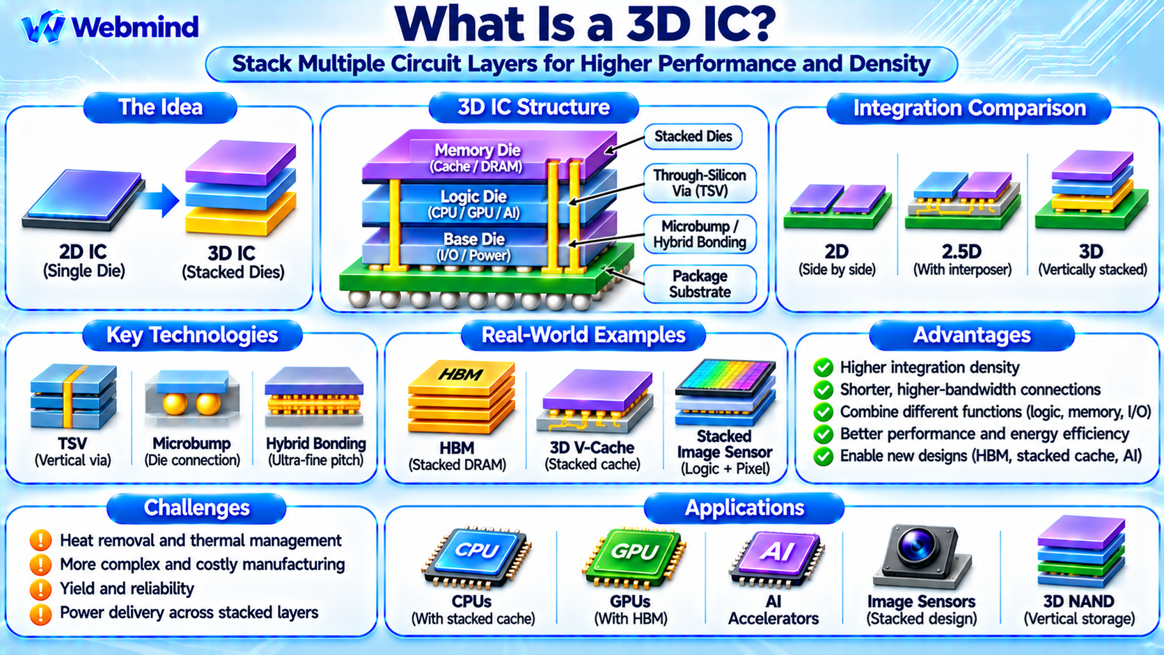
A 3D IC, or Three-Dimensional Integrated Circuit, is a semiconductor device that integrates multiple layers of electronic circuits vertically within a single chip or package.
Instead of placing all circuits side by side on one silicon die, 3D IC technology allows semiconductor dies or device layers to be stacked and interconnected.
This approach can increase integration density, shorten communication distances, and improve the bandwidth between computing and memory components.
3D IC technology is increasingly important in advanced processors, High Bandwidth Memory (HBM), artificial intelligence accelerators, and high-performance computing systems.
As conventional transistor scaling becomes more challenging and expensive, three-dimensional integration provides another way to improve semiconductor performance and functionality.
How Does a 3D IC Work?
A traditional integrated circuit contains transistors and metal interconnections fabricated primarily within one semiconductor die.
A 3D IC extends this concept by stacking multiple circuit layers or semiconductor dies vertically.
These layers communicate through specialized vertical electrical connections rather than relying entirely on longer horizontal connections.
For example, a computing die may be connected to a cache die stacked directly above it.
The two dies can exchange data through dense vertical interconnections, potentially providing higher bandwidth and shorter communication paths than conventional package-level connections.
Some 3D IC designs stack separately manufactured dies, while others build multiple device layers sequentially on the same wafer.
The exact structure depends on the manufacturing process and application.
Main Components of a 3D IC
A modern 3D integrated circuit may contain several important structures.
Semiconductor Dies: Individual silicon circuits containing processors, memory arrays, control logic, or specialized accelerators.
Vertical Interconnects: Electrical connections that carry signals and power between stacked semiconductor layers.
Through-Silicon Vias (TSVs): Conductive structures that pass through silicon to connect different layers.
Microbumps: Small conductive contacts used to connect neighboring semiconductor dies.
Hybrid Bonding: A bonding technology that combines dielectric bonding and fine-pitch metal connections.
Package Substrate: Provides electrical connections between the stacked dies and the external system.
Thermal Management Structures: Help transfer heat away from the semiconductor stack.
Different 3D IC technologies use different combinations of these components.
What Is a Through-Silicon Via (TSV)?
A Through-Silicon Via is a vertical electrical connection that passes through a silicon die or interposer.
TSVs are created by forming small holes in silicon, adding insulating and conductive materials, and connecting the resulting structures to circuit wiring.
They allow electrical signals to travel vertically between stacked semiconductor dies.
For example, HBM devices use TSVs to connect multiple DRAM dies in a vertical memory stack.
Compared with conventional connections around the edges of semiconductor packages, TSVs can provide shorter electrical paths and greater interconnection density.
However, TSV fabrication introduces additional manufacturing challenges, including alignment, mechanical stress, electrical parasitics, and wafer thinning.
What Is Hybrid Bonding?
Hybrid bonding is an advanced semiconductor bonding technique used to connect dies or wafers at extremely fine interconnect pitches.
It combines direct bonding between dielectric surfaces with electrical connections between corresponding metal contacts, commonly copper.
Unlike conventional microbump connections, hybrid bonding can support much smaller connection spacing.
This allows a large number of vertical connections within a limited area.
Hybrid bonding is used in selected advanced memory, image sensor, and processor technologies.
Its advantages include high interconnection density and potentially lower communication energy.
However, successful hybrid bonding requires extremely clean surfaces, precise alignment, and strict manufacturing control.
2.5D vs. 3D IC: What Is the Difference?
2.5D and 3D integration are closely related advanced packaging technologies, but they use different physical arrangements.
2.5D Packaging: Multiple dies are generally positioned side by side and connected through a high-density interposer or bridge structure.
3D IC: Two or more active circuit layers or semiconductor dies are stacked vertically and connected through specialized interconnects.
For example, a GPU positioned next to HBM stacks on a silicon interposer is commonly described as a 2.5D integration arrangement.
A processor die with an additional cache die stacked directly above it is an example of 3D integration.
These technologies can also be combined.
A 2.5D package may contain vertically stacked HBM devices, creating a system that uses both horizontal and vertical integration.
What Is Die-to-Die Stacking?
Die-to-die stacking involves joining individual semiconductor dies after they have been fabricated.
The dies are aligned and bonded using microbumps, hybrid bonding, or other advanced interconnection techniques.
One advantage is that individual dies can be tested before stacking.
This may reduce the risk of combining defective components.
However, stacking introduces additional manufacturing operations and reliability requirements.
Other approaches include wafer-to-wafer bonding and die-to-wafer bonding.
The best method depends on die size, manufacturing yield, alignment requirements, and production cost.
3D IC and High Bandwidth Memory
High Bandwidth Memory is one of the most important commercial examples of three-dimensional semiconductor integration.
HBM stacks multiple DRAM dies vertically and connects them through TSVs.
The stacked memory device communicates with a processor through a wide, high-speed interface, often supported by advanced packaging.
HBM provides very high aggregate memory bandwidth while reducing certain communication distances and energy costs.
This makes it particularly valuable for GPUs, AI accelerators, and high-performance computing systems.
However, HBM manufacturing requires sophisticated wafer processing, die stacking, thermal management, and testing.
The memory stack itself uses 3D integration, while its connection to a neighboring compute die may use 2.5D packaging.
3D IC and Stacked Cache
Three-dimensional integration can also increase cache capacity without requiring all cache memory to occupy additional area beside the processor cores.
For example, AMD’s 3D V-Cache technology uses vertically integrated cache dies in selected processor products.
The additional cache can increase the amount of data stored close to the CPU cores.
This may improve performance in workloads that benefit from larger cache capacity, such as certain games and computational applications.
However, a larger cache does not automatically improve every workload.
Performance also depends on cache latency, memory access patterns, processor architecture, and software behavior.
3D IC vs. Chiplet Technology
Chiplets are semiconductor dies designed to work together within a larger computing system.
3D IC technology describes an integration approach in which circuit layers or dies are stacked vertically.
The two concepts are related but not identical.
A chiplet-based processor may arrange multiple dies side by side on a package substrate.
A 3D chiplet design may stack selected dies vertically to increase integration density or reduce communication distances.
Advanced systems may combine both methods, placing some dies side by side while stacking others.
This gives chip designers greater flexibility in selecting manufacturing technologies and physical layouts.
Advantages of 3D IC Technology
Higher Integration Density: Vertical stacking allows additional circuitry to be integrated without proportionally increasing the package footprint.
Shorter Interconnections: Some communication paths can be shortened by connecting vertically adjacent dies.
High Bandwidth: Dense vertical connections can support large numbers of parallel signals.
Heterogeneous Integration: Logic, memory, sensors, and specialized circuits can be combined using different semiconductor technologies.
Improved System Flexibility: Designers can separate functions across different layers or dies.
Potential Energy Efficiency: Shorter and denser interconnects can reduce energy consumption for certain data transfers.
The actual benefits depend on architecture, manufacturing methods, and the physical arrangement of the circuits.
Challenges of 3D IC Technology
Despite its advantages, 3D integration introduces significant engineering challenges.
Thermal Management: Vertically stacked active dies can make heat removal more difficult, particularly for high-power processors.
Manufacturing Complexity: Advanced stacking requires precise alignment, bonding, thinning, and interconnection processes.
Yield: A defective die or bonding failure can affect the functionality of the complete stack.
Power Delivery: Electrical power must be distributed reliably across multiple layers.
Testing: Manufacturers must verify individual dies, vertical connections, and complete stacked systems.
Mechanical Stress: Different materials and temperature changes can introduce stress within the stack.
Cost: Advanced bonding equipment and additional fabrication steps can increase manufacturing expenses.
These challenges require coordinated improvements in chip design, manufacturing, packaging, and cooling technologies.
What Is Monolithic 3D Integration?
Monolithic 3D integration is an approach in which multiple transistor or circuit layers are fabricated sequentially on the same substrate.
Unlike conventional die stacking, which connects separately manufactured chips, monolithic integration builds additional device layers directly above previously fabricated structures.
This can enable very dense vertical interconnections.
However, upper-layer manufacturing must avoid damaging the circuits already formed below.
Temperature limitations, materials compatibility, alignment, and manufacturing yield are major challenges.
Monolithic 3D integration remains an important area of semiconductor research and development.
It should not be confused with conventional stacked-die packaging.
Where Are 3D ICs Used?
Three-dimensional integration is used in several important semiconductor applications.
High Bandwidth Memory: Stacks DRAM dies to achieve high memory capacity and bandwidth within a compact structure.
CPUs: Uses stacked cache or other vertically integrated components in selected processors.
AI Accelerators: Combines advanced memory and computing resources to improve system capabilities.
CMOS Image Sensors: Uses stacked semiconductor layers to separate pixel arrays from supporting logic and processing circuits.
3D NAND Flash: Builds multiple layers of memory cells vertically to increase storage density, although its monolithic layer construction differs from conventional stacked-die 3D ICs.
Advanced Chiplet Systems: Uses vertical integration to combine specialized semiconductor dies.
High-Performance Computing: Benefits from dense interconnections and advanced memory integration.
These applications demonstrate how vertical integration can extend semiconductor capabilities beyond conventional planar chip layouts.
The Future of 3D IC Technology
Three-dimensional integration is becoming increasingly important as semiconductor designers seek improvements beyond traditional transistor scaling.
Future systems may combine computing layers, cache memory, specialized accelerators, and high-bandwidth memory within advanced packages.
Hybrid bonding and other fine-pitch interconnect technologies are expected to support denser connections between stacked dies.
At the same time, thermal engineering, power delivery, design automation, and manufacturing yield will remain major challenges.
3D IC technology will likely coexist with conventional monolithic chips, chiplet architectures, and 2.5D packaging.
The most appropriate approach depends on performance requirements, cost, reliability, and system architecture.
Conclusion
A 3D IC is an integrated circuit system that uses vertically stacked semiconductor dies or circuit layers connected through specialized interconnect technologies.
Techniques such as TSVs, microbumps, and hybrid bonding make it possible to integrate multiple layers of computing and memory hardware.
3D integration can improve density, bandwidth, and system flexibility, but it also introduces challenges involving heat, manufacturing, power delivery, and reliability.
Technologies such as HBM, stacked cache, and advanced image sensors demonstrate the practical value of three-dimensional semiconductor integration.
Understanding 3D IC technology provides an important foundation for studying semiconductor packaging, chiplets, TSVs, hybrid bonding, HBM, advanced processors, and the future of integrated circuit manufacturing.