Introduction
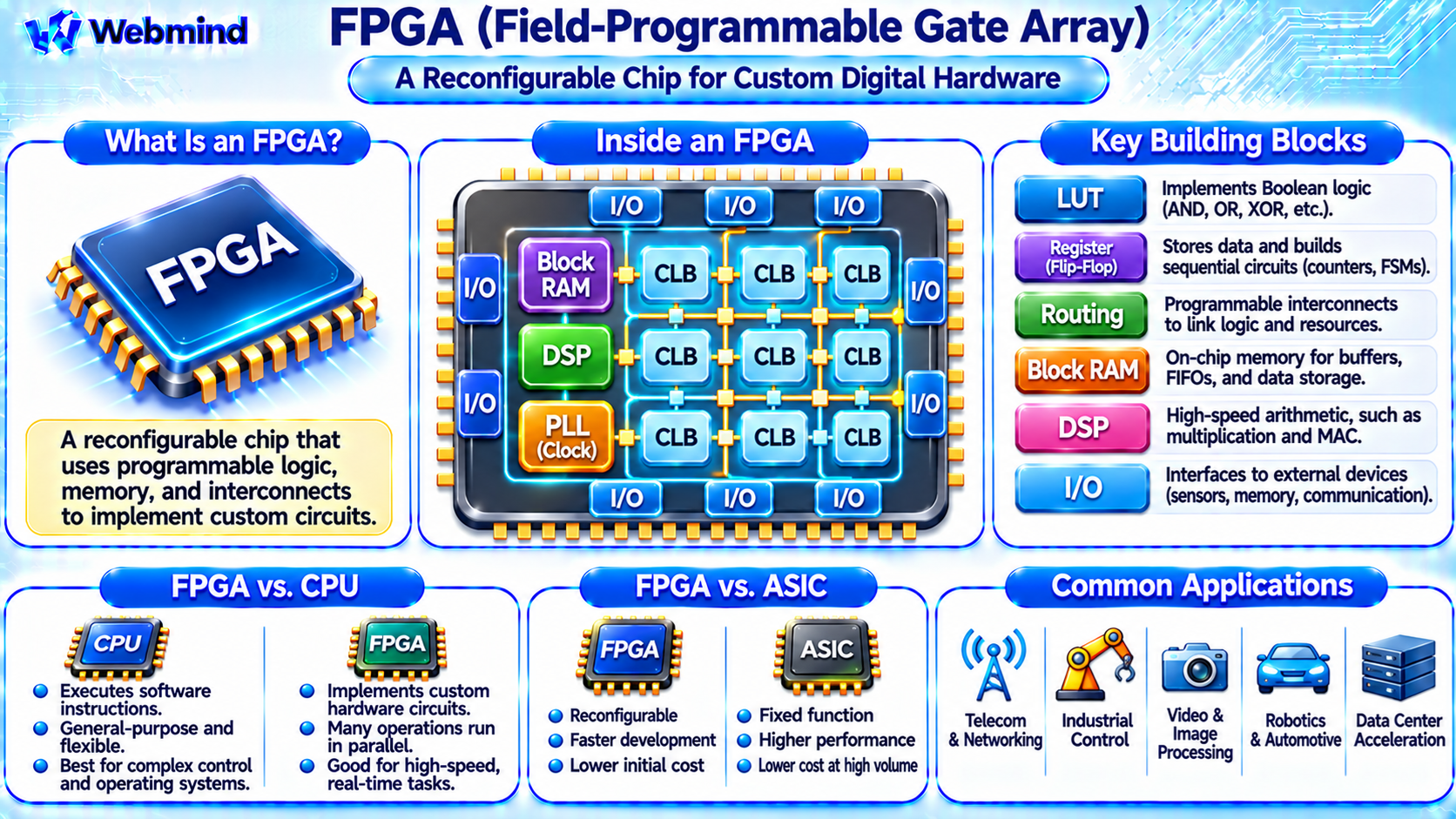
An FPGA, or Field-Programmable Gate Array, is a semiconductor device containing configurable digital logic, programmable interconnections, and specialized hardware resources.
Unlike a conventional processor that executes software instructions sequentially, an FPGA can be configured to implement custom digital circuits that operate in parallel.
The term field-programmable means that the device can be configured after manufacturing, often directly by the customer or developer.
FPGAs are widely used in embedded systems, telecommunications, industrial automation, robotics, aerospace, digital signal processing, and hardware acceleration.
They offer an important combination of hardware flexibility, parallel processing capability, and deterministic timing.
How Does an FPGA Work?
An FPGA contains physical hardware resources manufactured into the semiconductor chip.
These resources include logic elements, registers, programmable routing networks, memory blocks, and input/output interfaces.
The FPGA’s behavior is determined by configuration data, commonly called a bitstream.
When the bitstream is loaded into the FPGA, it configures the logic functions and the connections between hardware resources.
For example, the same FPGA can be configured as a digital counter, motor controller, communication interface, or signal-processing accelerator.
Unlike a CPU, which normally changes operations by executing different machine instructions, an FPGA changes its hardware functionality through configuration.
The resulting circuit can contain many independent operations running simultaneously.
Main Components of an FPGA
A modern FPGA contains several important building blocks.
Look-Up Tables (LUTs): Implement combinational Boolean functions such as AND, OR, XOR, multiplexers, and more complex logic expressions.
Flip-Flops and Registers: Store binary data and support sequential circuits, counters, pipelines, and state machines.
Programmable Routing: Connects logic blocks, memory resources, and other hardware components through configurable interconnections.
Block RAM (BRAM): Provides dedicated on-chip memory for data buffers, FIFOs, and other storage applications.
DSP Blocks: Perform arithmetic operations such as multiplication, addition, and multiply-accumulate calculations.
I/O Blocks: Connect the FPGA to external sensors, processors, memory devices, and communication interfaces.
Clock Management: Uses dedicated clock networks and resources such as PLLs or other clock-control circuits to distribute and manage timing signals.
Some advanced FPGAs also contain high-speed transceivers, memory controllers, processors, and specialized acceleration hardware.
What Is a LUT in an FPGA?
A Look-Up Table is one of the fundamental programmable logic resources inside an FPGA.
A LUT stores the output values of a Boolean truth table and selects the appropriate value according to its input signals.
For example, a two-input LUT has four possible input combinations and can store four output values.
To implement an AND gate, the LUT stores:
0, 0, 0, 1
To implement an XOR gate, it stores:
0, 1, 1, 0
The same physical LUT can therefore implement different Boolean functions by changing its configuration.
Modern FPGAs commonly use LUTs with multiple inputs, such as six-input LUTs, although the architecture varies by manufacturer.
How Do Registers Work in an FPGA?
Registers store binary information between clock events.
They are commonly implemented using flip-flops located near the FPGA’s programmable logic resources.
For example, a digital counter uses combinational logic to calculate the next count value and registers to store the current count.
At the appropriate clock edge, the registers capture the updated value.
Registers also allow designers to construct pipelines, improving the operating frequency of complex digital circuits.
Together, LUTs and registers form the foundation of many FPGA implementations.
What Is Programmable Routing?
Programmable routing connects different hardware resources inside an FPGA.
The device contains networks of wires and configurable switching structures.
The FPGA configuration determines which connections are enabled.
For example, the output of one LUT can be connected to another LUT, a register, or an output interface.
Programmable routing allows designers to build complex circuits from the same physical collection of hardware resources.
However, routing introduces electrical delay and consumes power, so placement and routing optimization are important aspects of FPGA development.
What Are Block RAM and DSP Blocks?
Modern FPGAs contain specialized resources that perform certain operations more efficiently than general-purpose logic.
Block RAM: Dedicated memory arrays used for buffers, FIFOs, lookup data, and temporary storage. Many FPGA architectures support configurable memory widths and dual-port access.
DSP Blocks: Dedicated arithmetic circuits designed for operations such as multiplication, addition, and multiply-accumulate processing.
For example, a digital signal-processing system can use DSP blocks to implement filters while Block RAM stores incoming samples.
Using dedicated resources reduces the amount of general-purpose LUT logic needed for these functions.
FPGA vs. CPU: What Is the Difference?
A CPU is a programmable processor that executes machine instructions according to its instruction set architecture.
An FPGA is a configurable hardware device that implements custom digital circuits.
CPU: Provides flexible, general-purpose instruction execution and is well suited to operating systems, applications, and complex control software.
FPGA: Implements hardware functions that can operate concurrently, making it useful for specialized processing, precise timing, and high-throughput data streams.
For example, a CPU may execute a software loop to process sensor samples.
An FPGA can implement a dedicated processing pipeline that accepts new samples at regular clock intervals.
However, FPGA designs are not automatically faster than CPU software. Performance depends on the algorithm, hardware architecture, memory bandwidth, and implementation quality.
FPGA vs. ASIC
An ASIC, or Application-Specific Integrated Circuit, is a semiconductor chip designed for a particular application.
An FPGA can be reconfigured after manufacturing, while a conventional ASIC has a fixed hardware implementation.
FPGA Advantages: Reconfigurability, shorter hardware development cycles, and lower initial manufacturing investment.
ASIC Advantages: Potentially better performance, lower power consumption, smaller silicon area, and lower unit cost at sufficiently high production volumes.
FPGAs are often used for prototyping, research, specialized equipment, and products requiring design flexibility.
ASICs are commonly preferred when production volume and performance requirements justify custom chip development.
How Is an FPGA Programmed?
FPGA developers commonly use Hardware Description Languages (HDLs), such as Verilog, SystemVerilog, or VHDL.
Unlike conventional programming languages used to describe a sequence of software operations, HDLs can describe hardware structures and concurrent behavior.
A typical FPGA development process includes several stages.
Design Entry: Describe the hardware using an HDL, schematic, or supported higher-level design method.
Simulation: Verify the circuit’s behavior before loading it onto hardware.
Synthesis: Convert the design into logic resources supported by the target FPGA.
Placement and Routing: Assign hardware functions to physical resources and configure their connections.
Timing Analysis: Check whether the circuit meets required clock and timing constraints.
Bitstream Generation: Create the configuration data for the FPGA.
Hardware Testing: Load the bitstream and verify operation on an FPGA development board.
Popular development environments include AMD Vivado and Intel Quartus Prime.
What Is an FPGA Bitstream?
A bitstream is configuration data used to establish the operating behavior of an FPGA.
Depending on the device architecture, it configures LUT functions, routing connections, I/O settings, and other programmable resources.
Many SRAM-based FPGAs load configuration data from external nonvolatile memory or a host system during startup.
Because SRAM configuration is volatile, these devices normally require reconfiguration after power is removed and restored.
Other FPGA technologies use flash-based or antifuse configuration methods with different persistence characteristics.
The bitstream does not replace the physical transistors inside the chip. Instead, it determines how the existing hardware resources operate and connect.
Why Are FPGAs Good at Parallel Processing?
One of the most important features of an FPGA is hardware parallelism.
A designer can create multiple circuits that operate simultaneously.
For example, an FPGA may read sensor data, filter incoming samples, perform arithmetic calculations, and transmit results through separate hardware pipelines.
These operations can overlap rather than being executed as one sequential software instruction stream.
FPGAs can also provide deterministic processing latency when designed with appropriate timing and buffering.
However, memory bandwidth, resource availability, clock frequency, and communication overhead still limit overall performance.
What Are SoC FPGAs?
A System-on-Chip FPGA combines programmable logic with processor cores and other integrated hardware.
For example, some SoC FPGA devices contain Arm processor cores alongside FPGA fabric.
The processor can run software, including an operating system, while the programmable logic implements specialized hardware functions.
The two parts communicate through internal interfaces.
This combination is useful in embedded systems because software can handle general-purpose control while FPGA hardware accelerates time-sensitive operations.
SoC FPGAs are commonly used in industrial equipment, communications, robotics, and advanced embedded applications.
Where Are FPGAs Used?
FPGAs are used across many industries.
Telecommunications: High-speed networking, packet processing, signal processing, and communication protocols.
Industrial Automation: Motor control, equipment monitoring, and deterministic hardware interfaces.
Robotics: Sensor processing, real-time control, and specialized hardware acceleration.
Aerospace and Defense: Signal processing, communication systems, and specialized embedded hardware.
Data Centers: Network acceleration, storage processing, and selected computational workloads.
Video Processing: Real-time image filtering, video pipelines, and camera interfaces.
Semiconductor Development: ASIC prototyping, hardware verification, and system validation.
Their flexibility allows engineers to implement specialized hardware without manufacturing a completely new integrated circuit.
Advantages of FPGAs
Reconfigurable Hardware: The same device can implement different digital circuits.
Parallel Processing: Multiple hardware operations can execute simultaneously.
Deterministic Timing: Dedicated circuits can provide predictable latency.
Rapid Prototyping: Developers can test and revise hardware designs without fabricating a new chip.
Specialized Resources: Block RAM, DSP blocks, and high-speed interfaces support complex applications.
Hardware Customization: Designers can create interfaces and processing architectures suited to specific requirements.
These advantages make FPGAs useful when hardware flexibility and specialized processing are important.
Limitations of FPGAs
Despite their capabilities, FPGAs also have disadvantages.
Development Complexity: Hardware design requires knowledge of digital logic, timing, and verification.
Power Consumption: Programmable routing and configuration structures may consume more power than equivalent optimized ASIC circuits.
Resource Limits: Designs must fit within the available LUTs, registers, memory blocks, and DSP resources.
Timing Challenges: Long logic paths and routing delays can reduce achievable clock frequency.
Cost: High-performance FPGAs can be expensive compared with simpler microcontrollers or high-volume ASICs.
Tool Complexity: FPGA development environments require synthesis, implementation, timing analysis, and hardware debugging.
These limitations influence whether an FPGA is the best choice for a particular application.
Conclusion
An FPGA is a reconfigurable semiconductor device that allows engineers to implement custom digital hardware using programmable logic and interconnections.
Its major building blocks include LUTs, registers, programmable routing, Block RAM, DSP blocks, I/O interfaces, and clock-management resources.
Unlike CPUs that execute software instructions, FPGAs implement dedicated circuits that can process information concurrently.
FPGAs are widely used in embedded systems, communications, robotics, digital signal processing, and hardware acceleration.
Understanding FPGAs provides an important foundation for studying Boolean algebra, logic gates, LUTs, sequential logic, Verilog, digital circuit design, and modern computer engineering.