Introduction
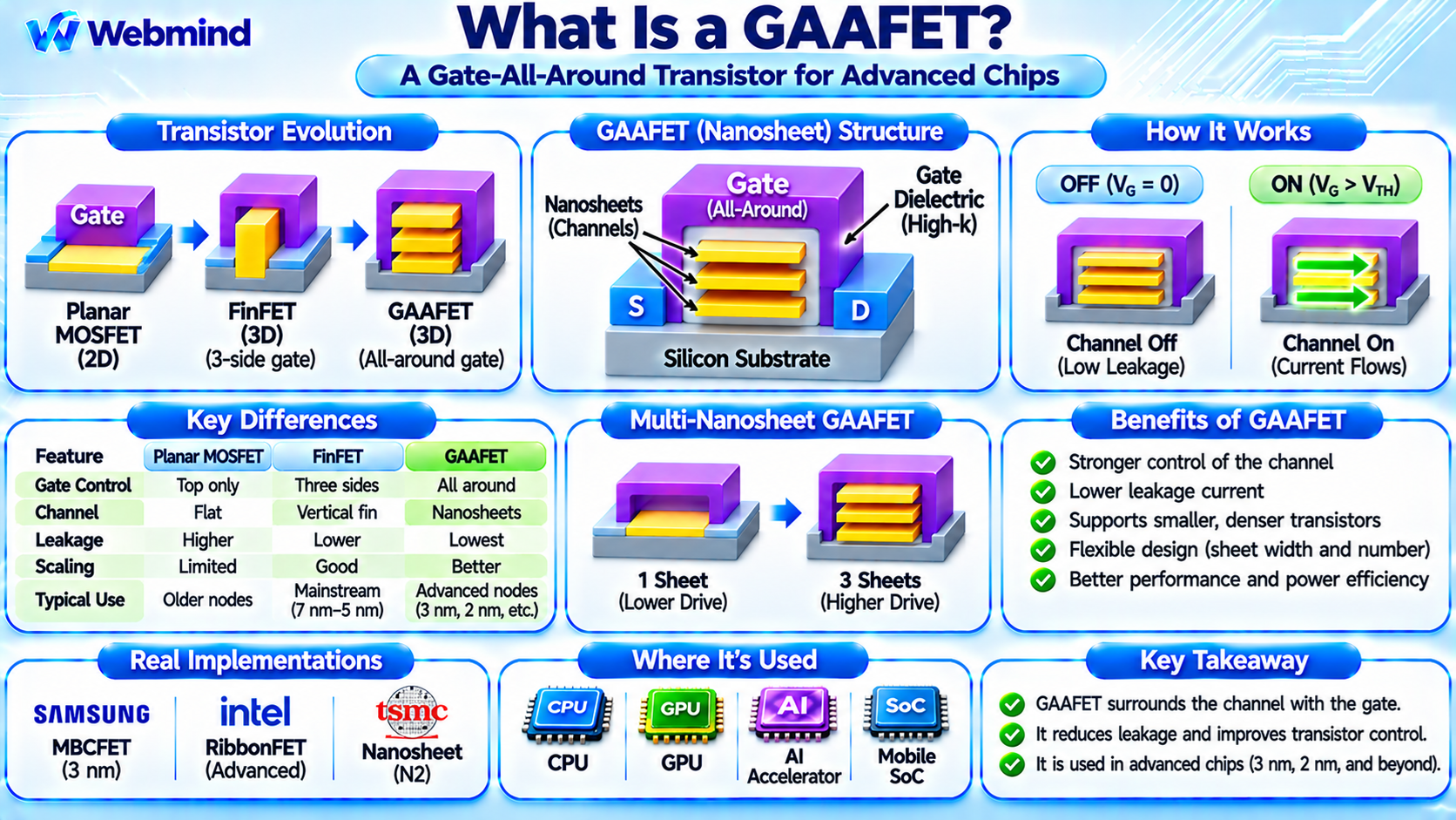
A GAAFET, or Gate-All-Around Field-Effect Transistor, is an advanced semiconductor transistor designed to improve electrical control, reduce leakage current, and support continued transistor scaling.
Unlike traditional planar MOSFETs and FinFETs, a GAAFET uses a gate structure that surrounds the semiconductor channel on all sides.
This provides stronger electrostatic control over the movement of electrical charge.
GAAFET technology represents an important development in modern semiconductor manufacturing.
It is being adopted in advanced logic processes used to manufacture high-performance processors, mobile chips, and other sophisticated integrated circuits.
As traditional transistor structures approach their practical scaling limits, GAAFETs provide a way to improve transistor density, performance, and energy efficiency.
How Does a GAAFET Work?
A GAAFET operates according to the same fundamental principle as a MOSFET: an electric field generated by the gate controls the conductivity of a semiconductor channel.
The transistor contains a source, drain, gate, and channel.
When an appropriate voltage is applied to the gate, a conducting channel allows current to flow between the source and drain.
When the gate voltage is reduced below the required operating threshold, the channel becomes much less conductive.
The defining feature of a GAAFET is that the gate surrounds the channel from all sides.
This structure improves control over the channel and helps suppress unwanted electrical effects that become increasingly significant as transistor dimensions shrink.
Main Components of a GAAFET
A modern GAAFET contains several important semiconductor structures.
Source: A semiconductor region connected to one end of the conducting channel.
Drain: The region connected to the opposite end of the channel.
Channel: A narrow semiconductor structure through which charge carriers move when the transistor conducts.
Gate Electrode: Surrounds the channel and controls its conductivity through an electric field.
Gate Dielectric: An insulating layer separating the gate electrode from the channel. Advanced devices typically use high-k dielectric materials.
Nanosheets or Nanowires: Thin semiconductor structures that form the conducting channels in many modern GAAFET implementations.
Isolation Structures: Electrically separate nearby devices and reduce unwanted interactions.
The exact geometry depends on the semiconductor manufacturing process and transistor design.
What Are Nanosheet Transistors?
A nanosheet transistor is a common implementation of GAAFET technology.
Instead of using one solid vertical fin, nanosheet transistors typically contain several thin semiconductor sheets stacked vertically.
The gate surrounds each sheet, allowing strong control over the conducting channels.
For example, a transistor may contain three vertically stacked nanosheets, each providing an additional path for electrical current.
Using multiple nanosheets increases the effective conducting channel width without requiring a proportional increase in the transistor’s footprint.
The width and thickness of the nanosheets can also be engineered to achieve different electrical characteristics.
This design provides additional flexibility compared with conventional FinFET structures.
GAAFET vs. FinFET: What Is the Difference?
FinFETs and GAAFETs are both three-dimensional field-effect transistors designed to improve electrical control over small semiconductor channels.
FinFET: Uses a vertical fin-shaped channel. The gate controls the channel from three sides.
GAAFET: Uses a channel that is surrounded by the gate on all sides.
The additional gate coverage allows GAAFETs to provide stronger electrostatic control, particularly at very small transistor dimensions.
FinFET transistor drive strength is commonly adjusted by changing the number of fins.
Nanosheet GAAFETs can offer greater flexibility through changes in nanosheet width and the number of stacked channels.
However, GAAFET manufacturing is more complex, and its advantages depend on the specific device structure, manufacturing process, and circuit requirements.
Why Is Gate-All-Around Control Important?
As transistor channel lengths decrease, the source and drain electric fields can interfere with the gate’s ability to control current.
These effects are known as short-channel effects.
They can increase leakage current, influence threshold voltage, and make transistor switching less predictable.
A gate-all-around structure improves the gate’s electrostatic influence over the channel.
This helps reduce short-channel effects and supports further device scaling.
Better channel control can also allow transistor designers to optimize operating voltage, performance, and leakage characteristics.
However, overall chip energy efficiency still depends on circuit architecture, interconnects, switching activity, and operating conditions.
How Are GAAFETs Manufactured?
GAAFET fabrication involves advanced semiconductor manufacturing techniques.
A typical nanosheet manufacturing process begins with alternating layers of semiconductor materials, such as silicon and silicon-germanium, grown on a wafer.
Lithography and etching define the required transistor structures.
Source and drain regions are formed, and selected sacrificial semiconductor layers are removed to release the nanosheet channels.
A gate dielectric and metal gate are then formed around the exposed nanosheets.
This creates the gate-all-around structure.
Additional processing forms electrical contacts, insulating layers, and metal interconnections.
The process requires precise control of nanosheet dimensions, selective etching, material deposition, and alignment.
These requirements make GAAFET manufacturing more challenging than conventional planar transistor fabrication.
GAAFET and Advanced Semiconductor Nodes
GAAFET technology is associated with the transition to increasingly advanced semiconductor manufacturing generations.
Samsung introduced its Multi-Bridge-Channel FET (MBCFET) technology in its 3 nm-class manufacturing process.
Intel has developed a nanosheet-based gate-all-around architecture called RibbonFET for its advanced manufacturing roadmap.
TSMC has introduced nanosheet transistor technology for its N2 process generation.
Although these technologies share the gate-all-around principle, their transistor geometries, materials, and manufacturing methods are not identical.
It is important to understand that process-node labels such as 3 nm and 2 nm do not directly represent the physical gate length or nanosheet thickness.
They are manufacturing technology designations rather than exact measurements of transistor dimensions.
GAAFET vs. Planar MOSFET vs. FinFET
Modern transistor technology has evolved through several important structural generations.
Planar MOSFET: Uses a relatively flat semiconductor channel controlled primarily from above by the gate.
FinFET: Uses a vertical fin-shaped channel, allowing the gate to control three sides.
GAAFET: Surrounds the channel with the gate on all sides, providing stronger electrostatic control.
Each development addresses challenges associated with smaller transistor dimensions.
However, newer transistor structures do not automatically replace older technologies in every application.
Planar MOSFETs remain important in many mature-node products, power electronics, and analog circuits.
FinFETs continue to serve a wide range of advanced digital applications.
GAAFETs are particularly important for selected leading-edge logic manufacturing processes.
What Is CFET? The Next Step Beyond GAAFET
CFET stands for Complementary Field-Effect Transistor.
A CFET architecture vertically stacks complementary NMOS and PMOS devices rather than placing them side by side in the conventional arrangement.
This approach has the potential to reduce the circuit area required for CMOS logic.
CFET concepts can use advanced transistor structures, including nanosheet-based devices.
However, CFET fabrication introduces significant challenges involving electrical isolation, manufacturing complexity, thermal management, and interconnections.
CFET is an active area of semiconductor research and development rather than a universal replacement for GAAFET technology.
Where Are GAAFETs Used?
GAAFET technology is primarily aimed at advanced logic semiconductor applications.
CPUs: Supports the development of high-performance processor cores and dense digital logic.
GPUs: Can be used in advanced graphics and parallel processing chips manufactured on compatible process technologies.
AI Accelerators: Enables highly integrated computing circuits for neural network processing and specialized arithmetic operations.
Smartphone SoCs: Supports power-efficient integration of CPUs, GPUs, NPUs, and other processing components.
Advanced ASICs: Provides transistor technology for specialized logic circuits requiring high density and competitive performance.
Future Semiconductor Platforms: May support additional improvements in transistor architectures and advanced computing systems.
The presence of GAAFETs in a particular product depends on the manufacturing process selected for that chip.
Advantages of GAAFETs
Improved Electrostatic Control: The gate surrounds the channel, reducing the influence of unwanted source and drain electric fields.
Reduced Short-Channel Effects: Better channel control helps manage leakage as transistor dimensions shrink.
Flexible Channel Design: Nanosheet width and stacking can be adjusted to optimize transistor characteristics.
Continued Transistor Scaling: GAAFETs support further improvements in density and performance at advanced manufacturing generations.
Potential Power Efficiency Improvements: Reduced leakage and optimized switching characteristics can improve energy efficiency in suitable designs.
Challenges of GAAFET Technology
GAAFETs also introduce significant engineering difficulties.
Complex Manufacturing: Forming and releasing nanosheet channels requires extremely precise fabrication processes.
Nanosheet Uniformity: Small variations in thickness and dimensions can influence transistor performance.
Parasitic Resistance and Capacitance: Advanced transistor structures require careful optimization of electrical connections.
Thermal Management: Heat removal becomes increasingly challenging in highly integrated transistor structures.
Manufacturing Cost: Advanced equipment, materials, process development, and verification increase production expenses.
Process Yield: Maintaining consistent transistor characteristics across large wafers is essential for economically viable manufacturing.
These challenges require improvements in materials engineering, lithography, etching, deposition, and semiconductor process control.
Why Are GAAFETs Important?
GAAFETs represent an important step in the evolution of semiconductor transistor architecture.
For decades, semiconductor manufacturers improved chip performance by reducing transistor dimensions and increasing integration density.
As planar MOSFET scaling became more difficult, FinFETs provided stronger channel control through three-dimensional structures.
GAAFETs extend this principle by surrounding the channel completely with the gate.
This makes them important for continued improvements in advanced logic manufacturing.
However, future computing performance will also depend on advances in chip architecture, memory systems, interconnect technology, chiplets, and semiconductor packaging.
Transistor scaling remains important, but it is only one part of modern semiconductor innovation.
Conclusion
A GAAFET is an advanced field-effect transistor that uses a gate-all-around structure to provide strong electrical control over a semiconductor channel.
Modern implementations commonly use stacked nanosheets, allowing engineers to optimize transistor drive current, leakage, and physical dimensions.
Compared with planar MOSFETs and FinFETs, GAAFETs provide improved electrostatic control and support continued scaling at advanced semiconductor manufacturing nodes.
Although manufacturing complexity remains a challenge, GAAFET technology is becoming an important foundation for future generations of high-performance and energy-efficient integrated circuits.
Understanding GAAFETs is essential for studying MOSFETs, CMOS technology, FinFETs, nanosheet transistors, semiconductor lithography, transistor scaling, and advanced chip manufacturing.