Introduction
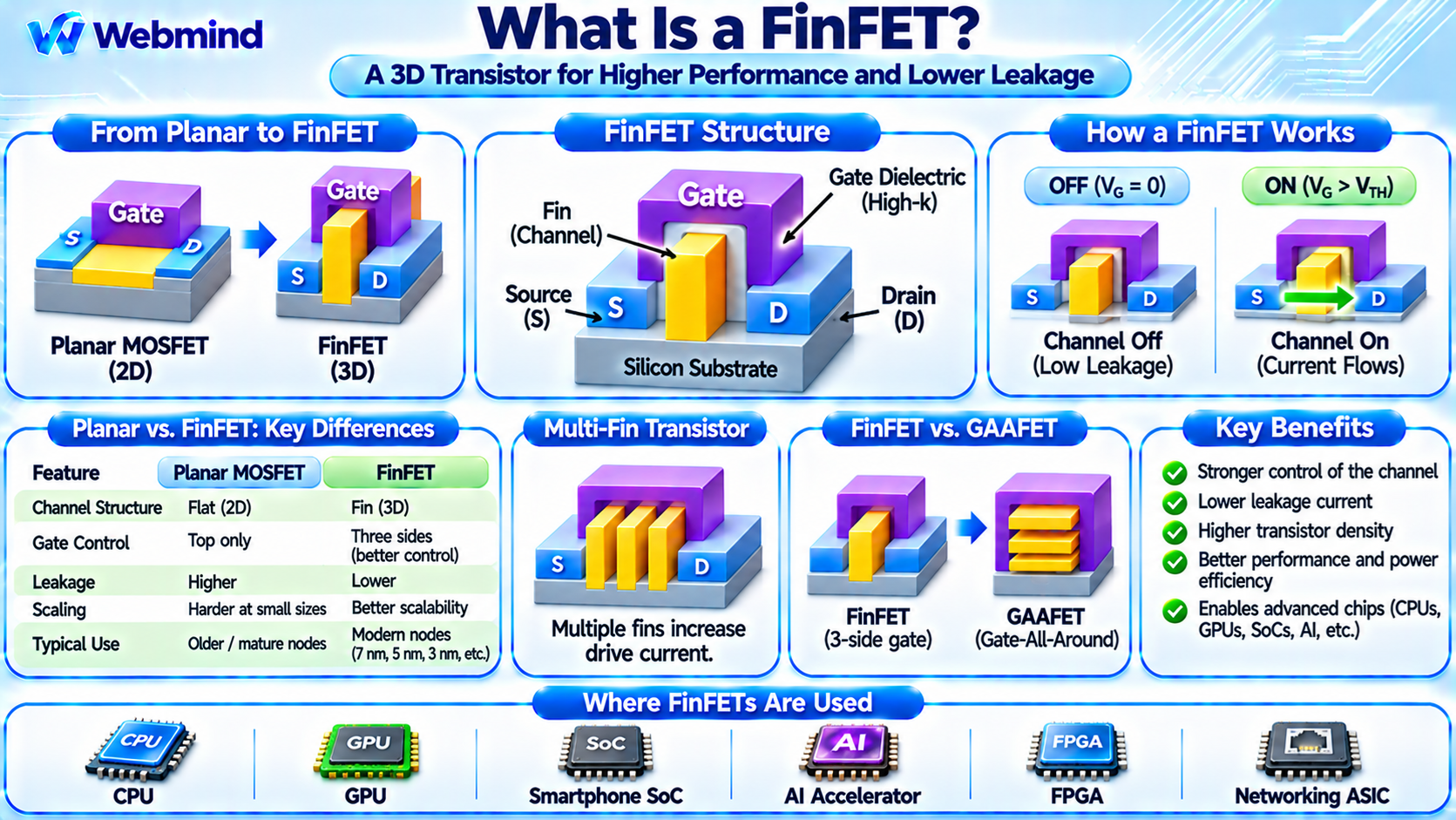
A FinFET, or Fin Field-Effect Transistor, is an advanced semiconductor transistor that uses a three-dimensional, fin-shaped channel to control electrical current.
It was developed to improve transistor performance and reduce leakage as semiconductor devices became smaller.
Unlike traditional planar MOSFETs, which have a relatively flat channel, a FinFET uses a narrow vertical silicon fin.
The gate wraps around multiple sides of the fin, providing better electrical control over the channel.
FinFET technology has played an important role in manufacturing modern CPUs, GPUs, smartphone processors, and Systems-on-Chip (SoCs).
It helped semiconductor manufacturers continue increasing transistor density while managing power consumption and short-channel effects.
How Does a FinFET Work?
A FinFET operates using the same fundamental field-effect principle as a conventional MOSFET.
The transistor contains a source, drain, gate, and semiconductor channel.
Applying an appropriate voltage to the gate changes the channel’s conductivity, controlling current flow between the source and drain.
The major difference is the channel structure.
In a planar MOSFET, the channel lies near the flat surface of the silicon substrate, and the gate primarily controls it from above.
In a FinFET, the channel forms within a narrow fin that rises vertically from the substrate.
The gate wraps around the top and two sides of the fin, creating a three-sided gate structure.
This provides stronger electrostatic control over the channel and helps reduce unwanted current leakage when the transistor is off.
Main Components of a FinFET
A FinFET contains several important semiconductor structures.
Silicon Fin: A narrow, vertical semiconductor structure that forms the transistor channel.
Gate Electrode: Controls the conductivity of the channel by generating an electric field.
Gate Dielectric: An insulating layer between the gate electrode and semiconductor channel. Advanced FinFETs commonly use high-k dielectric materials.
Source: One of the current-carrying regions connected to the transistor channel.
Drain: The other current-carrying region through which current flows when the transistor conducts.
Isolation Structures: Electrically separate neighboring transistors and reduce unwanted interactions.
Modern FinFET designs may also include engineered source/drain regions, metal gates, and other structures that improve device performance.
FinFET vs. Planar MOSFET
The main difference between FinFETs and traditional planar MOSFETs is how the gate controls the semiconductor channel.
Planar MOSFET: Uses a relatively flat channel with the gate positioned above it. This structure dominated semiconductor manufacturing for many decades.
FinFET: Uses a vertical fin-shaped channel, allowing the gate to control the channel from three sides.
As planar transistors became smaller, short-channel effects made it increasingly difficult to prevent leakage and maintain reliable switching.
FinFETs improved channel control, allowing manufacturers to continue scaling transistor dimensions.
However, FinFETs also require more complex fabrication processes than conventional planar MOSFETs.
What Are Short-Channel Effects?
Short-channel effects occur when transistor dimensions become small enough that the drain and source electric fields significantly influence channel behavior.
In traditional planar MOSFETs, these effects can make it difficult for the gate to control whether the transistor is on or off.
Common problems include increased leakage current, threshold-voltage variation, and drain-induced barrier lowering (DIBL).
DIBL occurs when increasing the drain voltage reduces the energy barrier that controls carrier movement through the channel.
FinFETs reduce many of these effects by surrounding more of the channel with the gate.
This stronger gate control helps maintain switching behavior as transistor dimensions decrease.
Why Are FinFETs More Energy Efficient?
FinFETs can improve energy efficiency by reducing unwanted leakage and supporting efficient transistor switching.
In digital circuits, transistors consume power during switching and through leakage currents when they are nominally off.
Improved electrostatic control allows FinFETs to reduce certain leakage mechanisms compared with similarly scaled planar transistors.
This can help semiconductor designers balance performance and power consumption.
However, a FinFET is not automatically more energy-efficient under every operating condition.
Actual power consumption depends on supply voltage, switching frequency, transistor dimensions, circuit architecture, and manufacturing technology.
What Is a Multi-Fin Transistor?
Some FinFET designs use multiple parallel fins controlled by a common gate.
Each fin provides an additional conducting channel, increasing the transistor’s effective channel width and current-driving capability.
For example, a transistor containing three fins can generally provide more drive current than a similar device containing one fin, assuming comparable operating conditions.
This approach allows circuit designers to select different transistor drive strengths.
However, fin-based designs can constrain transistor sizing because effective channel width is often adjusted in discrete increments rather than continuously.
These design considerations influence standard-cell libraries and advanced integrated circuit layouts.
How Are FinFETs Manufactured?
FinFET manufacturing requires highly precise semiconductor fabrication techniques.
The process begins with a silicon wafer and involves forming narrow fin structures through lithography and etching.
Isolation materials are introduced to electrically separate neighboring devices.
The gate structure is then formed around the fin, using carefully engineered dielectric and conductive materials.
Source and drain regions are created using doping and other processing techniques.
Finally, contacts and metal interconnections connect the transistors into functional circuits.
Modern FinFET manufacturing often uses advanced techniques such as high-k metal gates, self-aligned processing, and complex patterning methods.
These processes require extremely precise control over feature dimensions and alignment.
FinFET and Semiconductor Process Nodes
FinFETs became a major technology in advanced logic manufacturing during the transition beyond traditional planar transistor scaling.
Intel introduced FinFET-based Tri-Gate transistors in high-volume production at its 22 nm process generation.
Other major semiconductor manufacturers subsequently adopted FinFET technologies for advanced process nodes.
FinFETs became widely used in manufacturing generations commonly marketed as 16 nm, 14 nm, 10 nm, 7 nm, 5 nm, and 3 nm, although the specific transistor structures vary by manufacturer.
It is important to understand that process-node names do not directly describe the physical width of a fin or the exact length of a transistor gate.
They are technology-generation labels associated with a collection of manufacturing characteristics.
FinFET vs. GAAFET: What Is the Difference?
As semiconductor scaling continued, engineers developed Gate-All-Around Field-Effect Transistors (GAAFETs) to provide even stronger channel control.
FinFET: The gate surrounds three sides of a fin-shaped channel.
GAAFET: The gate surrounds the semiconductor channel on all sides.
Modern GAAFET implementations commonly use horizontally stacked nanosheets or nanowires.
The gate-all-around structure can improve electrostatic control and provide additional flexibility in transistor design.
GAAFET technology has begun replacing FinFETs in selected leading-edge manufacturing processes, although FinFETs remain important in many existing and advanced semiconductor products.
Both technologies are based on field-effect transistor principles and are used in modern CMOS circuit design.
Applications of FinFET Technology
FinFETs are widely used in advanced digital integrated circuits.
CPUs: Support high-performance processor cores, cache-related circuitry, and control logic.
GPUs: Enable dense parallel processing circuits used in graphics rendering and artificial intelligence.
Smartphone SoCs: Help integrate CPU cores, GPUs, AI accelerators, and communication functions within power-constrained devices.
AI Accelerators: Support highly integrated arithmetic circuits and specialized processing hardware.
Networking ASICs: Enable high-speed packet-processing and communication circuits.
FPGAs: Are used in certain advanced FPGA manufacturing processes to implement programmable logic and supporting circuitry.
FinFET technology has helped enable increasingly powerful chips while managing the challenges of transistor scaling.
Advantages of FinFETs
Improved Gate Control: The three-dimensional gate structure provides stronger control over the channel.
Reduced Leakage: FinFETs can reduce certain short-channel leakage effects compared with similarly scaled planar MOSFETs.
Higher Integration Density: FinFET technology supports continued scaling of digital integrated circuits.
Improved Performance: Advanced FinFET designs can provide favorable switching characteristics and drive current.
CMOS Compatibility: FinFETs can implement complementary NMOS and PMOS logic used in modern processors.
Limitations of FinFETs
Despite their advantages, FinFETs introduce several challenges.
Manufacturing Complexity: Creating narrow and uniform fins requires advanced lithography, etching, and process control.
Transistor Sizing Constraints: Drive strength is often adjusted through discrete numbers of fins.
Parasitic Effects: Three-dimensional device structures introduce capacitance and resistance challenges.
Thermal Management: Dense transistor integration can increase local power density and heat.
Continued Scaling Limits: As dimensions shrink further, maintaining electrostatic control and manufacturing consistency becomes increasingly difficult.
These challenges have encouraged the development of newer transistor structures, including GAAFETs.
Conclusion
A FinFET is a three-dimensional field-effect transistor that uses a vertical fin-shaped semiconductor channel and a gate that controls the channel from multiple sides.
Compared with traditional planar MOSFETs, FinFETs provide improved electrostatic control, helping reduce short-channel effects and support continued semiconductor scaling.
FinFET technology has been essential to modern CPUs, GPUs, smartphone processors, FPGAs, and advanced integrated circuits.
Although GAAFETs are increasingly used in selected leading-edge manufacturing processes, FinFETs remain a major semiconductor technology.
Understanding FinFETs provides an important foundation for studying MOSFETs, CMOS technology, transistor scaling, semiconductor manufacturing, GAAFETs, and modern chip architecture.