Introduction
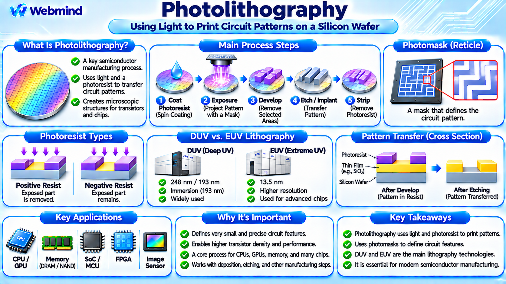
Photolithography is a semiconductor manufacturing process that uses light to transfer microscopic circuit patterns onto a silicon wafer.
It is one of the most important steps in producing integrated circuits, including CPUs, GPUs, memory chips, microcontrollers, and other semiconductor devices.
The process combines optical technology, light-sensitive chemicals, and precision manufacturing equipment to create extremely small patterns on a wafer surface.
Photolithography is closely related to lithography, but the term specifically emphasizes the use of light and photoresist to define patterns. These patterns are subsequently used in processes such as etching, deposition, and ion implantation.
How Does Photolithography Work?
Photolithography works by exposing a light-sensitive material called photoresist to a controlled pattern of light.
First, a silicon wafer is coated with photoresist. A lithography system then projects a circuit pattern from a photomask, also called a reticle, onto the coated wafer.
The exposed photoresist undergoes chemical changes. During development, selected regions dissolve and are removed, leaving a microscopic pattern.
This remaining photoresist pattern acts as a temporary mask for subsequent manufacturing operations.
For example, an etching process can remove material from areas not protected by photoresist, transferring the pattern into the underlying layer.
Photolithography therefore defines where semiconductor structures will be formed or modified rather than producing complete transistors directly.
Main Steps of the Photolithography Process
1. Wafer Cleaning and Preparation
Before applying photoresist, the wafer surface must be carefully cleaned to remove particles, moisture, and chemical contamination.
Even extremely small particles can interfere with pattern formation and reduce manufacturing yield.
Surface preparation may include dehydration baking and chemical treatments that improve photoresist adhesion.
2. Photoresist Coating
A liquid photoresist is applied to the wafer, commonly through spin coating.
During spin coating, the wafer rotates rapidly, spreading the liquid into a thin, relatively uniform film.
The photoresist thickness depends on the material, process requirements, and desired pattern dimensions.
After coating, the wafer usually undergoes a soft-bake process to remove excess solvent and stabilize the photoresist.
3. Mask Alignment and Exposure
A photomask contains the pattern that must be transferred onto the wafer.
Modern projection lithography machines use highly sophisticated optical systems to project the mask pattern onto the photoresist.
The machine carefully aligns the new pattern with existing circuit structures.
This alignment is essential because semiconductor chips contain many patterned layers that must connect accurately.
Light exposure changes the chemical properties of selected photoresist regions.
4. Post-Exposure Bake and Development
Some photoresist systems require a post-exposure bake to complete or control the chemical reactions initiated by exposure.
The wafer is then treated with a developer solution.
Depending on the photoresist type, either the exposed or unexposed regions are removed.
The remaining material forms the intended microscopic pattern.
5. Pattern Transfer
The developed photoresist serves as a temporary protective mask.
During etching, material can be removed from regions not covered by the resist.
In other processes, the resist pattern may define where dopants are introduced into the semiconductor.
The pattern-transfer method depends on the layer being manufactured and the overall chip design.
6. Photoresist Removal
After the required manufacturing operation, the remaining photoresist is removed using chemical or plasma-based processes.
The wafer is cleaned and prepared for the next fabrication stage.
These photolithography steps are repeated many times to construct the different layers of a semiconductor chip.
What Is Photoresist?
Photoresist is a light-sensitive chemical material used to create temporary patterns during semiconductor manufacturing.
Two major categories are commonly used.
Positive Photoresist: Exposed regions become more soluble in the developer and are removed during development.
Negative Photoresist: Exposed regions become less soluble, allowing them to remain while selected unexposed regions are removed.
Modern photoresists are carefully engineered for specific exposure wavelengths, pattern dimensions, and manufacturing conditions.
Their performance directly affects the accuracy of the printed circuit features.
What Is a Photomask?
A photomask is a patterned optical component that defines the circuit features to be transferred onto a wafer.
In conventional optical lithography, the mask contains regions that control how light passes through the pattern.
EUV lithography instead uses specialized reflective masks because extreme ultraviolet radiation is strongly absorbed by most materials.
Modern semiconductor chips require many masks to define different transistor and interconnect layers.
The accuracy of these masks is critical because even small patterning errors can affect the operation of the finished chip.
DUV vs. EUV Photolithography
Two important technologies used in semiconductor photolithography are Deep Ultraviolet (DUV) and Extreme Ultraviolet (EUV).
DUV Photolithography: Commonly uses wavelengths of 248 nm or 193 nm. Advanced 193 nm immersion lithography improves resolution by placing a liquid between the final optical element and the wafer.
EUV Photolithography: Uses approximately 13.5 nm light and specialized reflective optical systems operating in a vacuum.
EUV can print smaller features and reduce the number of patterning operations required for selected advanced chip layers.
However, DUV remains essential for many manufacturing steps, including layers that do not require EUV resolution.
Advanced semiconductor fabrication commonly uses both technologies.
What Is Overlay Accuracy?
Overlay accuracy describes how precisely a newly patterned layer aligns with structures formed during earlier manufacturing steps.
Modern semiconductor chips contain multiple layers of transistors, contacts, and metal interconnections.
If these layers are misaligned, electrical connections may fail or unwanted connections may occur.
Lithography systems therefore use precision measurement and alignment techniques to position patterns extremely accurately.
For advanced semiconductor processes, overlay requirements can be measured on the nanometer scale.
Overlay control is one of the most important factors affecting semiconductor manufacturing yield.
Photolithography vs. Etching
Photolithography and etching are closely related but perform different functions.
Photolithography defines the desired pattern in a light-sensitive photoresist layer.
Etching removes selected material from the underlying wafer layers according to that pattern.
For example, photolithography may create a pattern of narrow lines in photoresist.
An etching process then transfers that pattern into a deposited material layer.
Together, these processes allow manufacturers to construct microscopic electronic structures with precisely controlled dimensions.
Why Is Photolithography Important?
Photolithography determines the placement and dimensions of many critical structures inside integrated circuits.
Improved lithography resolution helps manufacturers increase transistor density and produce more complex chips.
However, smaller features require increasingly precise optics, advanced photoresist materials, accurate alignment, and sophisticated process control.
Photolithography is also expensive. Advanced lithography equipment, mask manufacturing, and process development represent major investments for semiconductor manufacturers.
Despite these challenges, photolithography remains essential to the continued development of high-performance computing, artificial intelligence, memory technology, and advanced electronics.
Applications of Photolithography
Photolithography is used throughout semiconductor and microfabrication industries.
CPUs and GPUs: Defines microscopic transistor structures and electrical interconnections.
Memory Chips: Supports the fabrication of DRAM, SRAM-related circuitry, and NAND Flash structures.
Microcontrollers and SoCs: Creates digital, analog, and mixed-signal integrated circuits.
FPGAs and ASICs: Enables manufacturing of configurable logic devices and application-specific chips.
Image Sensors: Defines pixel structures and supporting electronic circuits.
MEMS Devices: Creates microscopic structures used in accelerometers, pressure sensors, and other devices.
Photolithography is also used in selected photonic devices and other precision microfabrication applications.
Conclusion
Photolithography is a fundamental semiconductor manufacturing process that transfers microscopic circuit patterns onto silicon wafers using light and photoresist.
The process includes wafer preparation, photoresist coating, exposure, development, pattern transfer, and resist removal.
DUV and EUV technologies provide different levels of resolution and manufacturing capability, while accurate mask alignment and process control ensure reliable circuit fabrication.
Understanding photolithography provides an important foundation for learning semiconductor manufacturing, silicon wafers, transistors, CMOS technology, lithography equipment, and modern integrated circuit production.