Introduction
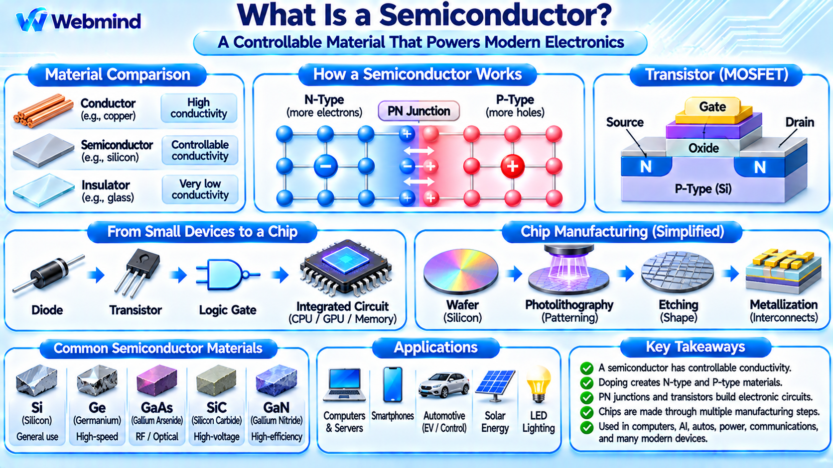
A semiconductor is a material whose electrical conductivity lies between that of a conductor, such as copper, and an insulator, such as glass.
Unlike ordinary conductors, the electrical properties of semiconductors can be precisely controlled through chemical doping, electric fields, temperature, and light.
Semiconductors are the foundation of modern electronics.
They are used to manufacture transistors, diodes, integrated circuits, CPUs, GPUs, memory chips, sensors, and power electronics.
Silicon is the most widely used semiconductor material, but other materials, including germanium, gallium arsenide (GaAs), silicon carbide (SiC), and gallium nitride (GaN), are important for specialized applications.
Understanding semiconductor technology helps explain how billions of transistors can operate together inside a modern computer chip.
How Does a Semiconductor Work?
The electrical behavior of a semiconductor depends on its atomic structure and the movement of electrical charge carriers.
In a pure silicon crystal, each silicon atom shares electrons with neighboring atoms through covalent bonds.
At low temperatures, relatively few electrons have enough energy to move freely through the material.
When energy is supplied, some electrons can move into states where they contribute to electrical conduction.
The absence of an electron in a normally occupied state behaves like a positively charged carrier called a hole.
Both electrons and holes can carry electrical current through a semiconductor.
The number and movement of these charge carriers determine the material’s electrical conductivity.
Engineers can modify semiconductor behavior by adding impurities or applying electric fields, allowing the creation of electronic switching and control devices.
What Is a Semiconductor Band Gap?
In solid-state physics, electrons occupy allowed ranges of energy called energy bands.
Two important energy bands are the valence band and the conduction band.
Valence Band: Contains electrons associated with atomic bonding in the material.
Conduction Band: Contains electronic states that allow electrons to move through the crystal and contribute to electrical conduction.
The energy difference between these bands is called the band gap.
In silicon, the band gap is approximately 1.12 electronvolts (eV) at room temperature.
Conductors generally have available electronic states that allow electrical current to flow easily. Insulators typically have large band gaps, making electrical conduction difficult.
Semiconductors have band gaps that allow their electrical behavior to be controlled under practical operating conditions.
Different semiconductor materials have different band gaps, which influence their suitability for logic circuits, optical devices, and power electronics.
What Are N-Type and P-Type Semiconductors?
Pure semiconductor materials can be modified through a process called doping.
Doping introduces carefully controlled amounts of impurity atoms into the semiconductor crystal.
N-Type Semiconductor
An N-type semiconductor is created by adding donor impurities, such as phosphorus or arsenic, to silicon.
These impurities provide additional electrons that can participate in electrical conduction.
Electrons are the majority charge carriers in N-type material.
P-Type Semiconductor
A P-type semiconductor is created by adding acceptor impurities, such as boron, to silicon.
These impurities increase the concentration of holes, which behave as positive charge carriers.
Holes are the majority carriers in P-type material.
Both N-type and P-type regions are essential building blocks for semiconductor devices.
What Is a PN Junction?
A PN junction is formed where P-type and N-type semiconductor regions meet.
When the two regions come into contact, electrons and holes diffuse across the boundary and recombine.
This creates a depletion region containing fixed ionized dopant atoms and an internal electric field.
The resulting potential barrier influences how electrical current flows through the junction.
When an appropriate forward voltage is applied, the barrier is reduced, allowing substantial current to flow.
Under reverse bias, the barrier generally increases, and only a small leakage current flows until breakdown conditions are reached.
PN junctions are fundamental to diodes, solar cells, photodetectors, and many types of transistors.
How Do Semiconductors Create Transistors?
A transistor is a semiconductor device used to control electrical current or voltage.
Two major transistor families are Bipolar Junction Transistors (BJTs) and Field-Effect Transistors (FETs).
Modern digital integrated circuits primarily use Metal-Oxide-Semiconductor Field-Effect Transistors (MOSFETs).
A MOSFET uses an electric field generated by its gate terminal to control current between the source and drain terminals.
In digital circuits, MOSFETs operate as electronic switches representing binary logic states.
A complementary MOS (CMOS) circuit combines NMOS and PMOS transistors to implement logic gates with relatively low static power consumption.
By connecting enormous numbers of transistors, engineers create logic gates, registers, arithmetic units, memory circuits, and complete processors.
Modern CPUs and GPUs can contain tens of billions of transistors.
How Are Semiconductor Chips Manufactured?
Semiconductor manufacturing involves transforming highly purified materials into complex electronic circuits.
The process begins with producing a high-purity silicon crystal, which is sliced into thin circular wafers.
Multiple fabrication stages are then used to create transistors and interconnections.
Photolithography: Transfers circuit patterns onto a wafer using light-sensitive materials and optical exposure systems.
Deposition: Adds thin layers of insulating, conducting, or semiconductor materials.
Etching: Selectively removes material to create the required structures.
Ion Implantation: Introduces dopant atoms into selected semiconductor regions.
Thermal Processing: Activates dopants and modifies material properties through controlled heating.
Metallization: Creates the conductive interconnections that link transistors and other circuit components.
These steps are repeated many times to build multiple layers of devices and wiring.
After fabrication, individual chips are tested, separated from the wafer, packaged, and prepared for use in electronic systems.
Common Semiconductor Materials
Different semiconductor materials offer different electrical and physical characteristics.
Silicon (Si): The dominant material for CPUs, memory chips, microcontrollers, and most digital integrated circuits.
Germanium (Ge): Used in selected high-speed devices, photodetectors, and silicon-germanium (SiGe) technologies.
Gallium Arsenide (GaAs): A compound semiconductor used in radio-frequency electronics, optoelectronics, and specialized high-speed devices.
Silicon Carbide (SiC): A wide-bandgap semiconductor used in high-voltage and high-temperature power electronics, including electric vehicle inverters.
Gallium Nitride (GaN): A wide-bandgap semiconductor used in efficient power converters, RF amplifiers, and certain optoelectronic devices.
The choice of material depends on voltage requirements, switching frequency, temperature, efficiency, manufacturing cost, and other design constraints.
Semiconductors vs. Conductors vs. Insulators
These three material categories differ primarily in how easily they conduct electrical current.
Conductors: Materials such as copper and aluminum contain mobile charge carriers and are commonly used for electrical wiring and interconnections.
Insulators: Materials such as glass and silicon dioxide strongly resist electrical conduction under ordinary conditions.
Semiconductors: Materials such as silicon have controllable conductivity, making them useful for electronic switches, amplifiers, sensors, and integrated circuits.
The ability to control semiconductor conductivity is what makes modern electronic devices possible.
Where Are Semiconductors Used?
Semiconductors are found in nearly every category of modern electronic technology.
Computers and Servers: CPUs, GPUs, memory chips, and supporting integrated circuits process and store digital information.
Smartphones: Application processors, wireless communication chips, sensors, and power-management circuits depend on semiconductor technology.
Artificial Intelligence: GPUs, NPUs, and specialized AI accelerators use semiconductor circuits to execute large numbers of calculations.
Automotive Electronics: Microcontrollers, sensors, power transistors, and communication devices support vehicle operation and electric power systems.
Industrial Automation: Semiconductor devices control motors, monitor equipment, process signals, and communicate between machines.
Solar Energy: Photovoltaic cells convert light into electrical energy using semiconductor junctions.
LED Lighting: Semiconductor materials emit light when electrons and holes recombine in suitable device structures.
Telecommunications: RF semiconductor devices support wireless communication, optical networks, and high-speed data transmission.
Why Are Semiconductors Important?
Semiconductors make it possible to integrate extremely large numbers of electronic components onto small chips.
Continued improvements in transistor design, manufacturing processes, and chip packaging have increased computing performance while reducing the energy required for many operations.
Semiconductor technology also supports advances in artificial intelligence, robotics, renewable energy, communications, and transportation.
However, manufacturing advanced chips requires highly specialized equipment, sophisticated design tools, expensive fabrication facilities, and complex global supply chains.
Modern semiconductor development therefore involves multiple disciplines, including physics, materials science, electrical engineering, computer architecture, and manufacturing technology.
Conclusion
A semiconductor is a material with controllable electrical conductivity that enables the operation of modern electronic devices.
By using doping, PN junctions, electric fields, and advanced fabrication techniques, engineers create transistors, diodes, sensors, and integrated circuits.
Silicon remains the foundation of most digital electronics, while materials such as SiC, GaN, and GaAs provide specialized capabilities for power, radio-frequency, and optical applications.
Understanding semiconductors is an essential foundation for studying transistors, logic gates, CPUs, GPUs, memory chips, FPGA and ASIC design, and modern semiconductor manufacturing.