Introduction
A memory controller is a hardware component responsible for managing communication between a processor and main memory, usually DRAM (Dynamic Random Access Memory).
It coordinates memory read and write operations, manages memory addresses, and ensures that data transfers follow the timing requirements of the memory system.
Modern CPUs, GPUs, microcontrollers, and Systems-on-Chip (SoCs) rely on memory controllers to access data efficiently.
In most modern desktop and server processors, the memory controller is integrated into the processor itself.
This design reduces communication overhead and allows the CPU to communicate with RAM without relying on a separate motherboard memory controller.
Memory controller performance is important because even a powerful CPU can spend substantial time waiting for data from memory.
How Does a Memory Controller Work?
When a processor needs information that is not available in its cache, the memory subsystem generates a request to retrieve the data from RAM.
The memory controller receives the request, determines the appropriate memory location, schedules the operation, and sends commands to the DRAM devices.
For example, suppose a CPU needs a value stored in system memory.
The processor first checks its cache hierarchy.
If the requested information is unavailable, a memory request travels through the processor’s internal interconnect toward the memory controller.
The memory controller translates the request into the necessary DRAM commands, observes memory timing restrictions, and retrieves the requested data.
The returned data is then transferred through the memory subsystem to the processor, often filling a cache line.
Memory writes follow a similar process, although write buffers and other mechanisms may allow writes to be scheduled independently of instruction execution.
Main Components of a Memory Controller
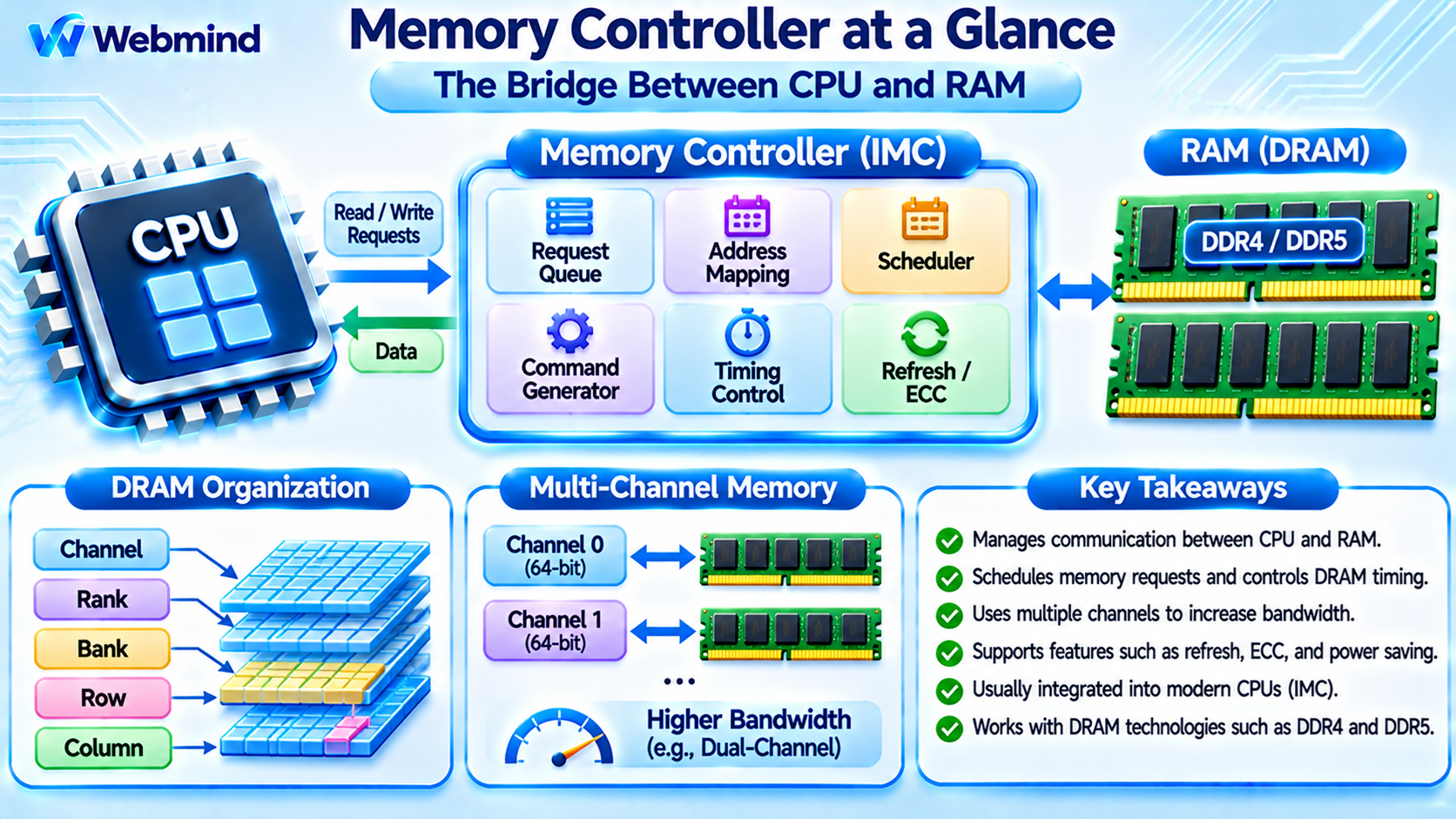
A modern memory controller typically contains several important functional blocks.
Request Queue: Temporarily stores memory read and write requests arriving from processor cores, caches, or other system components.
Address Mapping Logic: Converts physical memory addresses into the appropriate memory channel, rank, bank, row, and column information.
Memory Scheduler: Determines the order in which memory requests are processed. It attempts to balance performance, fairness, and DRAM timing constraints.
Command Generator: Produces DRAM commands such as activate, read, write, precharge, and refresh-related operations.
Timing Control Logic: Ensures that memory commands comply with timing parameters specified by the DRAM technology.
Refresh Management: Coordinates operations required to preserve data stored in DRAM cells.
Data Interface: Exchanges information with the memory physical interface, commonly called the PHY, which handles electrical signaling and timing at the memory connection.
Some memory controllers also support error correction, memory encryption, and advanced power-management features.
What Is an Integrated Memory Controller?
Older computer architectures commonly placed the memory controller in a separate chipset component, traditionally called the Northbridge.
The CPU communicated with this chipset, which then managed access to RAM.
Modern processors generally integrate the memory controller directly into the CPU or SoC.
This architecture is known as an Integrated Memory Controller (IMC).
An integrated controller can reduce memory access latency, improve available bandwidth, and simplify communication between processor cores and main memory.
In modern AMD and Intel processors, memory controllers are integrated into the processor package architecture.
Smartphone and embedded SoCs also typically integrate memory controllers alongside CPUs, GPUs, and other processing units.
However, the memory chips themselves may remain external to the processor or may be integrated into the same package, depending on the system design.
How Does DRAM Addressing Work?
DRAM is organized into a hierarchy of memory structures.
A typical DDR memory system may contain channels, ranks, banks, rows, and columns.
Channel: An independent memory communication interface connecting a memory controller to one or more memory devices.
Rank: A group of DRAM chips that operate together to provide a data interface of the required width.
Bank: An internal subdivision of DRAM containing arrays of memory cells.
Row: A group of memory cells activated together inside a bank.
Column: Identifies the portion of data accessed within an activated row.
Before accessing data, the memory controller may need to activate the appropriate row.
If the requested row is already active, the controller may access the data without another row activation. This is commonly called a row-buffer hit.
If a different row must be accessed, the controller may need to close the current row and activate another one, increasing access latency.
Efficient memory scheduling helps reduce unnecessary row operations and improves performance.
Memory Channels and Bandwidth
Memory controllers often support multiple memory channels to increase data transfer bandwidth.
For example, a conventional 64-bit DDR memory channel transfers 8 bytes of data per transfer, excluding additional bits used for certain error-correction configurations.
A DDR5-5600 channel operating at 5,600 million transfers per second provides a theoretical data bandwidth of:
5,600 MT/s × 8 bytes = 44.8 GB/s
A system with two independent channels of the same width and speed can theoretically provide 89.6 GB/s of aggregate bandwidth.
Actual performance is usually lower because of memory access patterns, timing constraints, protocol overhead, and system architecture.
DDR5 DIMMs also use two independent 32-bit subchannels per standard non-ECC module, improving memory access efficiency while maintaining the module’s overall 64-bit data width.
Memory channel count and organization are therefore important factors in system performance.
Memory Controller and RAM Timing
DRAM requires carefully coordinated timing between different operations.
Several timing parameters are commonly associated with DDR memory.
CAS Latency (CL): The delay, measured in clock cycles, between a column read command and the beginning of the corresponding data response.
tRCD: The minimum delay between activating a row and issuing an associated read or write command.
tRP: The minimum time required to precharge a bank before another row can be activated.
tRAS: The minimum time a row must remain active before it can be precharged.
The memory controller must respect these timing requirements to maintain reliable operation.
Higher memory transfer rates can increase bandwidth, but they do not automatically reduce the time required for every memory operation.
Memory performance depends on both bandwidth and latency.
Memory Controller vs. CPU Cache
The memory controller and CPU cache perform different functions.
CPU Cache: Stores copies of frequently accessed instructions and data close to processor execution units. Its purpose is to reduce the need for slower main-memory accesses.
Memory Controller: Coordinates actual communication with DRAM when memory requests must be serviced.
For example, if requested data is already present in L1 cache, the processor may complete the access without sending a request to the memory controller.
If the data is missing from the relevant cache levels, the memory subsystem may need to access RAM through the controller.
Cache efficiency therefore directly influences memory controller traffic and overall processor performance.
Memory Controllers in CPUs, GPUs, and SoCs
Different processing systems use memory controllers designed for their workloads.
CPUs: Modern desktop and server CPUs use integrated memory controllers to access DDR or other supported system memory technologies.
GPUs: Discrete graphics processors commonly use high-bandwidth memory controllers for GDDR or HBM. These controllers support the large data-transfer requirements of graphics rendering and parallel computing.
SoCs: Smartphone and laptop SoCs often integrate controllers optimized for LPDDR memory and power-efficient operation.
Microcontrollers: Many MCUs include controllers for internal SRAM and Flash memory. Some also contain external memory controllers for SDRAM, SRAM, or other memory devices.
FPGAs: FPGA devices may include dedicated memory controller hardware or configurable memory interface solutions for accessing external DDR memory.
The fundamental purpose remains the same: coordinating reliable and efficient access to memory.
Memory Controllers and ECC
ECC, or Error-Correcting Code, is used in certain memory systems to detect and correct memory errors.
A memory controller with ECC support can participate in generating and checking error-correction information during memory transfers.
A common ECC implementation corrects single-bit errors and detects many multi-bit errors.
ECC is particularly important in servers, workstations, and systems where data integrity is critical.
However, ECC support depends on the processor, memory controller, memory modules, and system configuration.
DDR5 also includes on-die ECC mechanisms within DRAM devices, which should not be confused with end-to-end system-level ECC memory protection.
Why Is the Memory Controller Important?
A memory controller directly affects memory bandwidth, latency, reliability, and energy efficiency.
An effective controller can improve performance by scheduling requests efficiently, exploiting memory bank parallelism, and reducing unnecessary DRAM operations.
In multicore systems, multiple CPU cores may compete for memory bandwidth. The controller must coordinate these requests while maintaining appropriate access priorities.
In AI accelerators and GPUs, memory bandwidth can become a major performance limitation because many processing units need large amounts of data simultaneously.
Modern memory controllers also use power-management techniques to reduce energy consumption when memory resources are idle.
However, a faster memory controller alone cannot eliminate every memory bottleneck. Cache behavior, application access patterns, memory technology, and system interconnects remain important.
Conclusion
A memory controller is an essential hardware component that manages communication between processors and main memory.
It translates memory requests into DRAM operations, schedules data transfers, enforces timing requirements, and coordinates refresh and other memory-management functions.
Modern integrated memory controllers support multiple channels, advanced memory technologies, and features such as ECC and power management.
Understanding memory controllers provides an important foundation for studying CPU architecture, DDR memory, computer performance, SoC design, GPU memory systems, and embedded hardware engineering.