Introduction
A PLL, or Phase-Locked Loop, is an electronic control system that synchronizes the phase and frequency of an output signal with a reference signal.
PLLs are widely used in CPUs, FPGAs, microcontrollers, communication systems, and high-speed digital electronics.
One of the most important applications of a PLL is clock generation.
A PLL can generate a higher-frequency or lower-frequency clock from a reference clock while maintaining a controlled relationship between the two signals.
For example, an FPGA may receive a 50 MHz clock from an external oscillator and use a PLL to generate a 100 MHz clock for internal logic.
PLLs are essential for clock management, frequency synthesis, signal synchronization, and many modern electronic systems.
How Does a PLL Work?
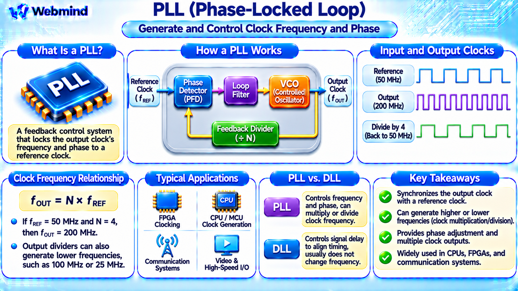
A PLL is a feedback control system that continuously compares a reference signal with a feedback signal derived from its own output.
If the signals are not aligned, the PLL adjusts its internal oscillator to reduce the phase difference.
This process continues until the output reaches a stable relationship with the reference signal.
When the PLL reaches this condition, it is said to be locked.
A typical PLL contains a phase detector, a loop filter, a controlled oscillator, and a feedback path.
These components work together to control the output frequency and phase.
Main Components of a PLL
Phase Detector
The phase detector compares the phase of the reference signal with the feedback signal.
It generates information indicating whether the feedback signal is leading or lagging behind the reference.
Many modern PLLs use a Phase-Frequency Detector (PFD), which can detect both phase and frequency differences.
Charge Pump and Loop Filter
In a common charge-pump PLL, the phase-frequency detector controls a charge pump.
The charge pump produces current pulses that are processed by a loop filter.
The loop filter smooths the control signal and influences the PLL’s response speed, stability, and noise characteristics.
Other PLL architectures may use different filtering and control methods.
Controlled Oscillator
The oscillator generates the PLL’s internal clock signal.
An analog PLL commonly uses a Voltage-Controlled Oscillator (VCO), whose frequency changes according to an applied control voltage.
Digital PLL architectures may use a Digitally Controlled Oscillator (DCO) or other digitally controlled timing structures.
Feedback Divider
A feedback divider reduces the oscillator frequency before the signal returns to the phase detector.
By controlling the divider ratio, the PLL can generate output frequencies that differ from the reference frequency.
How Does a PLL Multiply Clock Frequency?
One important function of a PLL is frequency multiplication.
In a simplified integer-N PLL, the reference frequency is compared with the oscillator output divided by N.
When the PLL is locked:
fVCO = N × fREF
For example, if the reference clock is 50 MHz and the feedback division ratio is 4, the oscillator frequency can be:
50 MHz × 4 = 200 MHz
An output divider may then reduce this frequency to another desired value.
For example, dividing 200 MHz by 2 produces a 100 MHz output clock.
Real FPGA PLLs may also include reference dividers, multiple output dividers, and fractional division capabilities.
The available frequencies depend on the device’s supported PLL operating ranges.
What Does PLL Lock Mean?
A PLL is locked when its feedback loop has established the required phase and frequency relationship with the reference signal within its operating tolerances.
During startup, the PLL generally requires time to stabilize.
This interval is called lock acquisition time.
Many FPGA PLLs provide a LOCKED output signal to indicate that the clock-generation circuit has reached its specified operating condition.
Digital logic may use this signal as part of its startup and reset sequence.
However, a LOCKED signal does not guarantee that every downstream circuit is operating correctly. Clock-domain timing and reset requirements must still be satisfied.
What Is Clock Jitter?
Clock jitter is the variation in the timing of clock edges relative to their ideal positions.
For example, a clock operating at 100 MHz has a nominal period of 10 nanoseconds.
In a real system, individual clock edges may occur slightly earlier or later than their ideal times.
This variation is called jitter.
PLLs can influence clock jitter because their oscillators, reference signals, and control loops introduce noise.
Depending on the loop design, a PLL may suppress some reference-clock noise while introducing additional oscillator-related noise.
Low jitter is especially important in high-speed communication, precision sampling, and timing-sensitive digital circuits.
What Is Phase Shift in a PLL?
A PLL can often generate clock signals with controlled phase relationships.
For example, an FPGA PLL may produce two clocks operating at the same frequency but with different phase offsets.
One clock may have a phase shift of 90 degrees relative to another.
Phase shifting can be useful for aligning data sampling with external signals or adjusting timing relationships between interfaces.
However, phase shift does not eliminate ordinary setup-time, hold-time, or clock-domain crossing requirements.
The available phase adjustments and their precision depend on the PLL architecture.
What Is a Fractional-N PLL?
A fractional-N PLL allows the effective feedback division ratio to have a fractional value.
This provides greater flexibility in generating output frequencies.
For example, a PLL may need to generate a clock frequency that cannot be obtained using a simple integer multiplication ratio.
Fractional division techniques can achieve a finer frequency resolution.
However, fractional-N PLLs introduce additional design considerations, including quantization effects, spurious signals, and phase noise.
They are widely used in frequency synthesizers and communication systems.
What Is the Difference Between PLL and DLL?
A DLL, or Delay-Locked Loop, is another electronic timing-control circuit.
A PLL adjusts the frequency and phase of an oscillator using feedback.
A DLL primarily adjusts the delay applied to a signal so that its output achieves a desired phase relationship with the reference.
PLL: Commonly used for frequency multiplication, frequency synthesis, and clock phase control.
DLL: Commonly used for clock alignment, delay adjustment, and timing compensation.
Both technologies are important in high-speed digital systems.
However, their implementations, capabilities, and limitations differ.
PLLs in FPGAs
Modern FPGAs contain dedicated clock-management resources, often including PLLs.
An FPGA development board typically supplies one or more reference clocks from external oscillators.
The FPGA can use PLL resources to generate the internal clock frequencies required by different parts of the design.
For example, a system may receive a 50 MHz reference clock and use a PLL to generate a 100 MHz processing clock and a 25 MHz peripheral clock.
FPGA PLLs may also support programmable phase shifts, clock compensation, and multiple clock outputs.
The exact capabilities depend on the FPGA manufacturer and device family.
Some architectures also provide related clock-management structures, such as Mixed-Mode Clock Managers (MMCMs).
PLLs and Clock Domains
A clock domain is a group of sequential circuits controlled by a particular clock.
An FPGA may contain multiple clock domains operating at different frequencies or phases.
For example, a processing circuit may operate at 100 MHz while a communication interface operates at 125 MHz.
Even when clocks are generated by the same PLL, their timing relationship must be considered carefully.
If data crosses between unrelated or asynchronous clock domains, special synchronization techniques may be required.
These techniques include synchronizer flip-flops, handshake circuits, and asynchronous FIFOs.
A PLL generates and manages clocks, but it does not automatically solve clock-domain crossing problems.
Why Not Use a Counter Instead of a PLL?
A digital counter can divide an existing clock frequency.
For example, a counter can generate a signal with half the input clock frequency.
However, an ordinary counter cannot directly generate a higher-frequency clock than its source clock.
A PLL can multiply frequency by controlling an internal oscillator.
PLLs can also provide phase adjustment and specialized clock-management functions.
In FPGA designs, clock generation should generally use dedicated clocking resources rather than ordinary combinational logic.
Counter-based enable pulses are often suitable when logic needs to operate less frequently without creating an additional clock domain.
PLLs in CPUs and Microcontrollers
Processors use clock-generation circuits to establish operating frequencies.
A CPU may receive a reference clock from an external oscillator or another clock source.
Internal PLL circuitry can generate higher-frequency clocks for processor cores and other functional units.
For example, a microcontroller may use a low-frequency external crystal oscillator and a PLL to generate a faster system clock.
Some devices allow software to configure PLL divider settings to select different operating frequencies.
Changing clock frequencies can influence performance, power consumption, and peripheral timing.
The clock system must remain within the electrical and timing limits specified by the device manufacturer.
PLLs in Communication Systems
PLLs are widely used in communication hardware.
Frequency Synthesis: Generate accurately controlled frequencies for transmitters and receivers.
Clock Recovery: Help recover timing information from received data streams in suitable clock-recovery architectures.
Radio Systems: Generate and stabilize frequencies used in modulation and demodulation.
High-Speed Serial Interfaces: Support clock generation and timing recovery in transceiver circuits.
Networking Hardware: Provide synchronized clocks for high-speed data communication.
Communication PLLs often have strict requirements for phase noise, jitter, frequency accuracy, and lock behavior.
These requirements can be more demanding than those of ordinary digital logic clock generators.
What Is PLL Bandwidth?
PLL bandwidth describes the range of frequency variations that the feedback loop can effectively track or respond to.
A wider loop bandwidth generally allows the PLL to respond more quickly to reference changes.
A narrower bandwidth may improve rejection of certain reference-related disturbances while allowing more oscillator noise to influence the output.
The actual behavior depends on the loop architecture and noise sources.
PLL bandwidth also affects stability and lock acquisition time.
Engineers must balance these characteristics when designing or configuring PLL circuits.
How Is a PLL Used in Verilog?
In FPGA development, a PLL is usually implemented using dedicated hardware resources rather than ordinary Verilog logic gates.
FPGA design tools commonly provide clock-generation IP blocks or configuration utilities.
The designer specifies the reference clock frequency, required output frequencies, phase settings, and other supported parameters.
The development software generates the necessary configuration and interface files.
A Verilog design can then connect to the PLL’s clock outputs and status signals.
The synthesis and implementation tools map the PLL configuration to the FPGA’s dedicated clock-management hardware.
Designers must also provide correct timing constraints for generated clocks and connected logic.
Advantages of PLLs
Frequency Multiplication: Generate clocks operating faster than the reference frequency.
Frequency Division: Produce lower-frequency clocks through supported divider structures.
Phase Control: Generate controlled phase relationships between clock signals.
Clock Synchronization: Maintain a defined relationship between output and reference signals.
Multiple Clock Outputs: Many FPGA PLLs can generate several related clocks.
Flexible Clock Management: Support different operating frequencies within the device’s specified limits.
These capabilities make PLLs essential in modern digital electronics.
Limitations of PLLs
PLLs also introduce important engineering challenges.
Lock Acquisition Time: The circuit requires time to stabilize after startup or configuration changes.
Jitter and Phase Noise: Real PLL outputs contain timing variations.
Operating Range Restrictions: Reference, oscillator, and output frequencies must remain within supported limits.
Power Consumption: PLL circuitry consumes additional electrical power.
Clock-Domain Complexity: Multiple generated clocks may require careful timing analysis and synchronization.
Configuration Requirements: Incorrect divider or phase settings can cause unreliable operation.
These limitations must be considered when designing high-speed digital systems.
Conclusion
A Phase-Locked Loop is a feedback control system that synchronizes the phase and frequency of an output signal with a reference signal.
PLLs use components such as phase detectors, loop filters, controlled oscillators, and feedback dividers to generate and stabilize clock signals.
They are widely used in CPUs, microcontrollers, FPGAs, communication systems, and high-speed electronic interfaces.
In FPGAs, PLLs provide essential clock-management capabilities, including frequency multiplication, division, and phase adjustment.
Understanding PLLs provides an important foundation for studying clock signals, FPGA architecture, digital timing, jitter, clock-domain crossing, and modern electronic system design.